Facebook
 Google
 GitHub
 Linkedin
The Benefits of 3Level Topologies in Combination with 7th Generation IGBT Technology
Over the past few months, SEMIKRON has introduced 950V and 1200V Generation 7 IGBTs from two different manufacturers.
Over the past few months, SEMIKRON has introduced 950V and 1200V Generation 7 IGBTs from two different manufacturers. Both Generation 7 IGBTs have undergone fundamental improvements since their predecessors were introduced. Thanks to the new chip design, the chip size is an average of 25 % smaller across all current classes. This allows for higher nominal currents in existing module housings, resulting in higher current density and an approximately 20% reduction in saturation voltage Vce,sat.
Another important new feature in Generation 7 IGBTs is the ability to operate at higher junction temperatures. The maximum junction temperature remains at Tj,max=175°C, with continuous operation permissible up to Tj,op=150°C. What is new, however, is that short-term operation at between 150°C and 175°C for up to one minute with a duty cycle of 20% is now possible. In this way, for example, a one-minute long inverter overload of 110% can be covered without the need for additional design reserves.

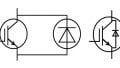
Figure 1: NPC and ANPC topology
This new chip generation allows for compact inverters with unprecedented power density. Especially the new 950V IGBTs, in a variant for high switching frequencies as well as a variant with optimized Vce,sat, are ideally suited for use in 3-level topologies up to 1500VDC.
3-Level topologies for 1500VDC solar applications
In 1500VDC applications, the most common topologies are Neutral Point Clamp (NPC) and Active Neutral Point Clamp (ANPC). Compared to the NPC, the ANPC has two additional switches that result in a higher degree of freedom but requires two additional drivers for T5 and T6 (Figure 1).
Different switching modes exist for the ANPC. Two popular switching modes are (Figure 2):
- High Frequency/Low Frequency (HF/LF) switching mode
- Low Frequency/High Frequency (LF/HF) switching mode

Figure 2: ANPC LF/HF and HF/LF switching mode
Both switching modes are different in the way the input and output stage is operated. In LF/HF mode, the input stage switches at the low switching frequency. In general, this equals the mains frequency, i.e. 50/60Hz. In contrast, the output stage switches at high frequency in the kilohertz range. The HF/LF mode is operated the opposite way. The different switching modes result in differences in the commutation loops. The commutation loops and the consequences for the phase leg design are shown and compared in Figure 3 and Figure 4.
Commutation Loops ANPC LF/HF (Figure 3):
Input stage: Low-frequency commutation occurs within half the input stage (small loop area).
Output stage: High-frequency commutation occurs between the input and output stages (large commutation area). A high gate resistance is required to minimize overvoltage.
Consequences: the phase leg circuit should be restricted to one power module to minimize the long commutation loop, or the phase leg should be split across two power modules, with all the switches of the same commutation loop kept inside the same package.

Figure 3: Commutation loops ANPC LF/HF
Commutation Loops ANPC HF/LF (Figure 4):
Input stage: High-frequency commutation occurs within half the input stage (small loop area). Low gate resistance possible.
Output stage: The low-frequency commutation occurs between the input and output stages (large commutation area). A Large gate resistance to minimize the overvoltage is acceptable since switching frequency is low.
Consequences: The phase leg can be designed within one module, two split modules or three half-bridge modules.

Figure 4: Commutation loops ANPC HF/LF
The decision as to which of the NPC, ANPC HF/LF or ANPC LF/HF topologies is best suited for a given application depends primarily on the available chip technology, the power factor range, and the switching frequency. For example, the 950V Generation 7 IGBT combined with SiC devices is the perfect match for high switching frequencies in photovoltaic (PV) and energy storage applications (ESS).
New 950V Generation 7 IGBTs
SEMIKRON uses the new Generation 7 IGBTs in different chip variants and housings. In the 950V class, two different chip variants are available: The “L7” version is optimized for minimum conduction losses, i.e. minimum Vce,sat, and should be used wherever long current lead times and only a few switching operations occur, e.g. in the LF stage of ANPC topologies. In contrast, the “S7” variant, which is optimized for minimum switching losses, is perfect for HF components. Plus, 950V IGBTs display better performance than 1200V IGBTs. As a general rule of thumb, IGBTs of lower nominal voltage also have lower switching losses. At the same time, a 950V blocking voltage is sufficient to support applications designed for 1500VDC.
Split ANPC Topology with SiC MOSFETs and 950V Generation 7 IGBTs
The first module housing to be discussed is the SEMITOP E2 in Split ANPC topology, optimized for LF/HF switching mode (Figure 5): one phase leg is divided into two SEMITOP E2 modules. The components that form one commutation loop are located in the same module to minimize the commutation inductances.
The L7 950V IGBT (low VCE,sat) is used in the input stage of the LF/ HF ANPC, switching at the mains frequency. In this case, the output stage consists of extremely fast switching SiC MOSFETs and SiC Schottky diodes. These allow for switching frequencies of 40 kHz and higher. With its 200A rating, the combination achieves an output power of up to 200kW with an excellent efficiency of >99% on full PCB-based system designs. Further paralleling of power modules is not required.
The second SEMIKRON module that uses this new chip technology is the MiniSKiiP 3 MLI (Figure 6). This 3-level NPC module is based entirely on silicon components and contains a full phase-leg at a rated current of 400A. Like the SEMITOP E2, this version uses L7 950V IGBTs with low VCE,sat for the slow switching positions, whereas the S7 high-speed IGBTs are used for the fast switches.

Figure 5: Split ANPC topology and SEMITOP E2 power modules. The commutating components are all within the same module
Comparing NPC and ANPC in the Applications
PV applications are mostly operated at power factors PF or cos phi of 0.8 to 1.0. This means the energy flow is unidirectional, from the solar panels through the inverter to the grid. In the NPC topology, the outer switches T1 and T4 generate predominantly switching losses, operating at higher switching frequencies (S7 IGBTs). The inner switches T2 and T3 generate mainly conduction losses (L7 IGBTs).

Figure 6: Full NPC Phase-leg in MiniSKiiP MLI 400A
Applications with bidirectional energy flow, such as energy storage systems, require chipsets that are optimized for the entire power factor range. During battery charging the energy flows from the grid to the inverter with PF=-1, while energy flows from the inverter to the grid with PF=1 when the battery is discharging. In contrast to the NPC, in the ANPC topology, the commutation path does not change with changing power factor and can serve the full power factor range. SEMIKRON also offers an ANPC solution for this in the MiniSKiiP 3 package with Icnom=400A.
Figure 7 compares the efficiency of an NPC and ANPC HF/LF module versus the power factor, both modules optimized for PV applications. At PF=1, the NPC has the same efficiency as the ANPC-HF/LF owing to the fact that the commutation loops and the active chips at this operating point are identical.
As soon as the PF gets smaller than 1, the NPC drops in efficiency due to switching losses in the inner switches T2/T3. Performance-wise, the ANPC-HF/LF shows the highest efficiency over the full power factor range. But this comes at the price of two additional switches and drivers. In light of this, and bearing in mind the 0.8…1 power factor range in PV applications as well as easier control, the NPC can be a good alternative to the ANPC-HF/LF.
Both variants achieve an output power of up to 200kW in full silicon or up to 250kW in hybrid SiC with SiC Schottky diodes used at position D5/D6 in NPC topology. For a higher power output, these modules can also be connected in parallel, which allows for interleaved operation with resulting output frequencies >30 kHz without the use of costly SiC components.

Figure 7: Efficiency over power factor for NPC and ANPC HF/LF
3-Level Topologies for High Power Applications
Three-level topologies also deliver clear advantages in high-power converters, i.e. 500kW to the multi-megawatt wind and solar power applications. On one hand, the efficiency is significantly increased thanks to the use of the latest Generation 7 IGBT technology and the lower blocking voltage of the IGBTs. In a wind turbine, this will reduce the semiconductor losses by about 38%. On the other hand, the voltage range specified in the Low Voltage Directive, which allows for system designs of up to 1000VAC and 1500VDC, can be fully exploited. This enables significant system cost reductions thanks to the lower overall current coupled with up to 40% lower cable losses or lower cabling cost.
For these high power applications, the use of 1200V components is necessary owing to the voltage reserve required during switching.
The introduction of the SEMITRANS 10 MLI 1200A in 2017 was an important milestone for SEMIKRON in PV inverter applications. The chip shrinkage accomplished in Generation 7 IGBTs led to the addition of the SEMITRANS 10 MLI 1400A to the portfolio. This module not only increases efficiency and current rating. In fact, thanks to optimized clamping diodes, it is now also possible to use this module over the full power factor range from -1 to +1. This is essential for wind power applications, where the generator-side inverter is always operated with a negative power factor.
Comparing Different NPC Designs for High Power Applications
In addition to the SEMITRANS 10 MLI, 3-level NPC topologies can also be created using standard half-bridge modules. Taking 1 MW design as an example, the following paragraph outlines the advantages and disadvantages of these designs in detail (see figure 8).
SEMITRANS 10 MLI, 2 Modules Per Phase Leg
This variant is the only one that allows for the NPC topology to be used with two modules only, resulting in the maximum power density. In addition, this design only requires two driver boards and a simplified DC bus connection of only three layers. A further advantage lies in the operation at power factors below 1. Since the commutation loop is only spread across two modules with a stray inductance of about 60nH, this design is key for fast switching and thus reduced losses.
The low commutation inductance is possible because both the DC laminates and the AC connection overlap. A further advantage of this solution is the current distribution to the AC terminals of both phase leg modules, which significantly reduces the thermal stress on the terminal connection.
SEMiX 3 Press-Fit half-bridge, 6 modules per phase leg: To cover the same power range as the SEMITRANS 10 MLI, a minimum of six SEMiX 3 Press-Fit modules (1200V / 600A) is necessary, resulting in the need for more gate drive elements, too. The physical arrangement of the modules per phase prevents an overlapping of DC and AC potentials, which limits the achievable commutation inductance of the NPC circuit. This has a particular effect on generator operation and results in extremely high inductance value of more than 200nH when commutating across three modules at negative power factor operation. In applications such as wind power or ESS, this makes the use of this module combination somewhat critical and means a high output power derating is needed. In addition, the paralleling of modules might require pre-selected modules or AC-chokes in order to reduce the current imbalance among the modules.

Figure 8: Comparison of NPC topologies featuring SEMITRANS 10 MLI, SEMiX 3 Press-Fit half-bridge and SEMITRANS 10 half-bridge
SEMiX 3 Press-Fit Half-Bridge, 6 Modules Per Phase Leg
To cover the same power range as the SEMITRANS 10 MLI, a minimum of six SEMiX 3 Press-Fit modules (1200V / 600A) is necessary, resulting in the need for more gate drive elements, too. The physical arrangement of the modules per phase prevents an overlapping of DC and AC potentials, which limits the achievable commutation inductance of the NPC circuit. This has a particular effect on generator operation and results in extremely high inductance value of more than 200nH when commutating across three modules at negative power factor operation. In applications such as wind power or ESS, this makes the use of this module combination somewhat critical and means a high output power derating is needed. In addition, the paralleling of modules might require pre-selected modules or AC-chokes in order to reduce the current imbalance among the modules.
SEMITRANS 10 Half-Bridge, 3 Modules Per Phase Leg
As with the SEMiX 3 Press-Fit, a 3-level NPC circuit can also be designed using standard SEMITRANS 10 half-bridge modules. Here, too, commutation takes place over 3 modules, but the linear arrangement of the DC and AC terminals allows for an overlapping bus bar design. Doing so results in a leakage inductance of about 100nH for the longest commutation path
In addition to the NPC topologies shown above, an ANPC HF/LF topology can also be achieved based on standard half-bridge modules. As mentioned above in relation to MiniSKiiP modules, this has the advantage that the commutation path is the same independent from the power factor. In the HF/LF version, fast commutation takes place inside a single module, which leads to a low commutation inductance of only 24nH in the SEMITRANS 10 package. One disadvantage of this solution, however, is the greater space requirements for the 3modules in comparison to the SEMITRANS 10 MLI, as well as the higher complexity of the control, gate driver and DC-link connection
The new 7th generation IGBT chips have led to further improvements in power density for 3-level applications. This applies to PCB-based systems in which the new generation 7 950V IGBTs are used as well as to high-power applications featuring 1200V components. With the different 3-level topologies having their own advantages and disadvantages, both the topology and the corresponding chipset have to be selected on the basis of the given application and the required operating point. The SEMITRANS 10 MLI achieves optimum performance, power density and system costs in the multi-megawatt wind and solar power applications in particular.
About the Authors
Bernhard Eichler received his degree in electrical engineering at Regensburg University of Applied Sciences, then MBA at International University of Applied Sciences Bad Honnef · Bonn. He worked as a senior manager product management medium voltage at SEMIKRON, which is one of the world's leading manufacturers of power modules and systems primarily in the medium output range (approx. 2 kW up to 10 MW). Our products are at the heart of modern energy-efficient motor drives and industrial automation systems. Further application areas include power supplies, renewable energies (wind and solar power) and electric vehicles (private cars, vans, buses, lorries, forklift trucks, and more). SEMIKRON's innovative power electronic products enable our customers to develop smaller, more energy-efficient power electronic systems. These systems, in turn, reduce global energy demand.
Andreas Giessmann received his degree in the field of electrical drives and controls at the University of Applied Sciences Dresden (HTW Dresden), then master of science in energy management at Hochschule für Technik und Wirtschaft Dresden (HTW Dresden). He worked as a senior application engineer at SEMIKRON, which is one of the world's leading manufacturers of power modules and systems primarily in the medium output range (approx. 2 kW up to 10 MW). Our products are at the heart of modern energy-efficient motor drives and industrial automation systems. Further application areas include power supplies, renewable energies (wind and solar power) and electric vehicles (private cars, vans, buses, lorries, forklift trucks, and more). SEMIKRON's innovative power electronic products enable our customers to develop smaller, more energy-efficient power electronic systems. These systems, in turn, reduce global energy demand.
- Andreas has a acco