Facebook
 Google
 GitHub
 Linkedin
Negative Capacitance Could Bring More Efficient Transistors
This article discusses the property called 'Negative Capacitance' which could bring more efficient transistors.
Researchers have experimentally demonstrated how to harness a property called negative capacitance for a new type of transistor that could reduce power consumption, validating a theory proposed in 2008 by a team at Purdue University.
The researchers used an extremely thin, or 2-D, layer of the semiconductor molybdenum disulfide to make a channel adjacent to a critical part of transistors called the gate. Then they used a “ferroelectric material” called hafnium zirconium oxide to create a key component in the newly designed gate called a negative capacitor.
Capacitance, or the storage of electrical charge, normally has a positive value. However, using the ferroelectric material in a transistor’s gate allows for negative capacitance, which could result in far lower power consumption to operate a transistor. Such an innovation could bring more efficient devices that run longer on a battery charge.
Hafnium oxide is now widely used as the dielectric, or insulating material, in the gates of today’s transistors. The new design replaces the hafnium oxide with hafnium zirconium oxide, in work led by Peide Ye, Purdue’s Richard J. and Mary Jo Schwartz Professor of Electrical and Computer Engineering.
“The overarching goal is to make more efficient transistors that consume less power, especially for power-constrained applications such as mobile phones, distributed sensors, and emerging components for the internet of things,” Ye said.
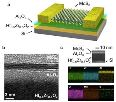
Figure 1. A new type of transistor (a) harnesses a property called negative capacitance. The device structure is shown with a transmission electron microscopy image (b) and in a detailed “energy dispersive X-ray spectrometry” mapping (c). Credit: Purdue University/Mengwei Si
Findings are detailed in a research paper published on Dec. 18 in the journal Nature Nanotechnology.
The original theory for the concept was proposed in 2008 by Supriyo Datta, the Thomas Duncan Distinguished Professor of Electrical and Computer Engineering, and Sayeef Salahuddin, who was a Purdue doctoral student at the time and is now a professor of electrical engineering and computer sciences at the University of California, Berkeley.
The paper’s lead author was Purdue electrical and computer engineering doctoral student Mengwei Si. Among the paper’s co-authors are Ye; Ali Shakouri, the Mary Jo and Robert L. Kirk Director of Purdue’s Birck Nanotechnology Center and a professor of electrical and computer engineering; and Muhammad A. Alam, the Jai N. Gupta Professor of Electrical and Computer Engineering, who made critical and wide-ranging contributions to the theory describing the physics behind negative capacitance devices.
Transistors are tiny switches that rapidly turn on and off, enabling computers to process information in binary code. Properly switching off is of special importance to ensure that no electricity “leaks” through. This switching normally requires a minimum of 60 millivolts for every tenfold increase in current, a requirement called the thermionic limit. However, transistors that harness negative capacitance might break this fundamental limit, switching at far lower voltages and resulting in less power consumption.
New findings demonstrate the ferroelectric material and negative capacitance in the gate results in good switching in both the on and off states. The new design achieves another requirement: for the transistors to switch on and off properly they must not generate a harmful electronic property called hysteresis.
The negative capacitance was created with a process called atomic layer deposition, which is commonly used in industry, making the approach potentially practical for manufacturing.
The research is ongoing, and future work will explore whether the devices switch on and off fast enough to be practical for ultra-high speed commercial applications.
“However, even without ultrafast switching, the device could still have a transformative impact in a broad range of devices that may operate at lower frequency and must operate with low power levels,” Ye said.
Portions of the research were based at the Birck Nanotechnology Center in Purdue's Discovery Park. The work was funded by the U.S. Air Force Office of Scientific Research, National Science Foundation, Army Research Office and Semiconductor Research Corporation.
The work was performed by researchers from Purdue, the National Nano Device Laboratories in Taiwan, and National Laboratory for Information Science and Technology of Tsinghua University in Beijing.
ABSTRACT
Steep Slope Hysteresis-free Negative Capacitance MoS2 Transistors
Mengwei Si1,3, Chun-Jung Su2, Chunsheng Jiang1,4, Nathan J. Conrad1,3, Hong Zhou1,3, Kerry D. Maize1,3, Gang Qiu1,3, Chien-Ting Wu2, Ali Shakouri1,3, Muhammad A. Alam1 and Peide D. Ye*,1,3
- School of Electrical and Computer Engineering, Purdue University, West Lafayette, Indiana 47907, United States
- National Nano Device Laboratories, Hsinchu 300, Taiwan
- Birck Nanotechnology Center, Purdue University, West Lafayette, Indiana 47907, United States
- Tsinghua National Laboratory for Information Science and Technology, Institute of Microelectronics, Tsinghua University, Beijing 100084, China
This article originally appeared in the Bodo’s Power Systems magazine.