Facebook
 Google
 GitHub
 Linkedin
Looking Back and Forward on 10 Years with GaN Systems
Back in the dark days after the internet bubble burst, Nortel had demised, and high tech in Canada’s Silicon Valley North was in the doldrums. The idea
Back in the dark days after the internet bubble burst, Nortel had demised, and high tech in Canada’s Silicon Valley North was in the doldrums. The idea of starting a semiconductor company based on an unknown technology probably seemed an insane idea. But that’s exactly what my partner John Roberts and I did. John was a fifty year veteran of the semiconductor business; I a serial entrepreneur with some half-dozen start-ups and IPOs to my credit. Recognizing those were our strengths and we weren’t about to learn new ones at this stage in our careers, we created GaN Systems. That was nearly ten years ago, and this September John and I announced our retirement from the company that has become the leader in gallium nitride power transistors.
What an amazing journey – not only building the company, but watching an entirely new technology evolve and become an established part of the power electronics world. Our timing was right. The world was awakening to the need for more efficient power management – the cleantech revolution was underway. The need for new core-enabling technologies – batteries, storage systems, more efficient electronics was evident. We saw the potential for wide bandgap technology to move from LEDs and RF applications to power switching devices – if only the design challenges could be overcome. And what challenges they turned out to be! Only a career overcoming the hurdles of high tech development (and funding!) gave us the vital element of perseverance to keep pursuing the goals.
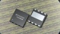
I’m often asked how a small unfunded semiconductor start-up in Canada could rise to the position of the pre-eminent supplier of a new technology in a field dominated by giants. I believe there are three main reasons. First, we approached the problem with a clean sheet of paper. We had no CMOS design heritage to adapt, no foundry to keep busy – just a lifetime of semiconductor knowledge to bring to bear. We quickly realized traditional layouts simply couldn’t handle the currents and switching speeds that gallium nitride portended. The result was our Island Technology, which solved all the problems of electromigration, inductance, scalability and yield. Later on we overcame the inductive limitations of traditional packaging by introducing our innovative embedded packaging, GaNPX – a bold move for a young start-up.
Second, we had access to a wide bandgap foundry - a rarity in those days. Operated by our local National Research Council labs and acquired from the ashes of Nortel, it offered a small, three inch GaN-on-SiC capability accompanied by a wealth of cooperative expertise. And third, the people. Out of chaos comes opportunity - high tech had collapsed in the area – but had left behind a wealth of technologists only too happy to be involved in something new and exciting. We were joined by material scientists, semiconductor process engineers, R&D directors and product managers of a caliber and experience a start-up could only dream of attracting. My role as CEO was easy – simply to provide the happy corporate environment to allow these great people to deliver their best – and they did!
Of course with any new technology there were naysayers, convinced that all we were attempting was impossible – defects would kill the devices, lateral devices couldn’t handle high currents, etc. Fortunately imagination and perseverance exists to defeat such views. A lot of time in the early years was on missionary work – explaining to anyone who would listen about the potential of gallium nitride. It was during this time that I came to meet my peers and fellow industry evangelists – Alex at EPC, Umesh and Primit at Transphorm, AJ and Dan at RFMD, – never really competitors, more collegial advocates of GaN’s future. I met visionary editors too, especially Bodo, who believed in GaN as a future technology and creatively aided the awareness process. It’s been a great and rewarding experience working alongside these folks – people with a lifetime of experience in power semiconductors – which I didn’t have - a spirit I’ve not encountered in my previous technologies.
As well as good device design, we had to build the supply chain to deliver the goods. Here too, the missionary work continued, persuading suppliers they needed to be on board when GaN arrived. Our early devices were normally-on GaN-on-SiC, followed by cascode development. But it was our partnership with TSMC, initiated some four years ago, that brought us to the point in 2014 where we launched into distribution the industry’s first family of normally-off, high-current GaN-on-Si devices.
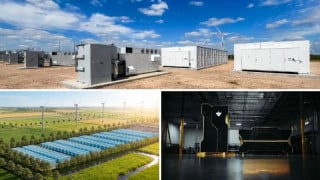
Since that launch, the rate of increases in GaN applications has been amazing to watch. By 2016 we were seeing commercial systems where GaN has enabled reductions of 4-10x in power system size, weight and power loss. The really exciting part has been the emergence of undreamed of applications enabled by GaN. We knew all along that as well as the obvious applications, GaN would trigger the imagination of bright application engineers and produce innovative new topologies and end-products undreamed of when we started. Today, we see this occurring in industrial, datacenter, consumer and particularly in automotive markets. This is one of the most rewarding aspects of what we have achieved. Our accomplishments were epitomized in the memorable day spent at the Google Little Box Challenge finals – eventually won by CE+T’s Red Electrical Devils team who used our devices to design the tour de force inverter which produced a power density of 143 W/cubic inch in a mere 14 cubic inches.
With the launch of our product family in 2014 it was time to transition the company to a full-scale semiconductor manufacturer, and again, with the backing of our unstintingly supportive VCs, we brought in the world-class team that would head this up. The company is in great hands for the future.
It has been an amazing journey, watching an entire new technology come from concept to full realization. John and I leave it with a mélange of emotions that range from the satisfaction of what has been achieved, to the excitement as we watch future applications unfold and see that we really did contribute to global conservation.