Facebook
 Google
 GitHub
 Linkedin
Simplify Power Electronics Design with GaN Power ICs
This article highlights Gallium Nitride's (GAN) advantages over silicon in terms of performance to finally displace silicon in power devices.
Early forms of Gallium Nitride (GaN) power devices required complex, expensive and frequency-limiting external circuits and complex packaging to protect and manipulate vulnerable gates, which severely restricted market adoption.
The introduction of monolithically-integrated GaN Power ICs, with drive, logic, and FET on a single die is the enabling step forward. This powerful merging of signal-to-power provides a rugged solution that is easy to use and greatly simplifies overall system design. This article highlights some of the past difficulties with early GaN, presents new GaN Power ICs, and shows high-frequency converter design examples that utilize this new and revolutionary technology to create applications with benchmark efficiency, power density, and low system cost.
AllGaN™ and GaN Power Integrated Circuits
Gallium Nitride (GaN) is a wide bandgap material that allows high electric fields so high carrier density can be achieved. A two-dimensional electron gas (2-DEG) with AlGaN/GaN heteroepitaxy structure gives very high mobility in the channel and drain drift region so resistance is much reduced compared to both Si and SiC. Creating lateral device structures achieves extremely low charge, for high-speed operation and also allows integration.
AllGaN™ is the industry’s first GaN Power IC Process Design Kit (PDK) which allows monolithic integration of 650V GaN IC circuits (drive, logic) with GaN FETs. Other functions can also be included, such as hysteretic digital input, voltage regulation, and ESD protection – all in GaN (see figure 1 for construction and integration). This monolithic integration of drive and switch is impossible using vertical GaN, dMode GaN or SiC.

Figure 1: AllGaN lateral structure ( Left ), integration of FET, driver, logic ( Right )
AllGaN Gate Solution: Easy to Drive
The earliest GaN power devices were dMode (depletion mode) which meant that they needed an additional Si FET in ‘cascode’ to keep them off, with subsequent negative results in packaging inductance and cost. Later, eMode (enhancement mode) GaN discrete devices had vulnerable gates and a very low threshold voltage. This made them very susceptible to noise and voltage spikes due to high-frequency and high dv/dt noise from the surrounding switched-mode converter circuit so required complex and expensive control and gate drive circuits (see figure 2 left). Additionally, both implementations restricted the high-frequency performance of the GaN switch, to the point where there was minimal, if any, an advantage over Si, so limiting market adoption.

Figure 2: Early GaN gate drive ( Left ), GaN Power IC ( Right )
Within the AllGaN solution, the GaN FET gate is driven safely, precisely and efficiently by the upstream integrated GaN driver. Simple, robust, low-current 3.3V, 5V or 15V signals, from standard, low cost, low voltage ‘no driver’ control ICs are fed directly into the GaN Power IC for an easy, low component count design (see figure 2 right ).
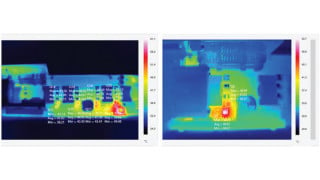
The waveforms exhibit a true “textbook” feeling with very clean rising and falling edges, no ringing, and extremely fast turn-ON and turn-OFF propagation delays (see figure 3). Integration eliminates gate overshoot and undershoots, while zero inductance on-chip insures no turn-OFF loss. This lack of ringing/overshoot makes tight control of deadtime easy in half-bridge circuits.
This exceptional level of fast and quiet switching performance, together with the integrated gate drive and simple PWM input, allows for the design of a variety of different high-frequency power converters, raising practical speeds more than 10x from 65/100kHz to 1MHz+.

Figure 3: Comparative waveforms for (upper) Si driver, discrete GaN FET vs. (lower) integrated GaN Power IC.
Easy Electrical and Mechanical Layout of GaN Power ICs
In high-frequency discrete designs, more design time is required to investigate and remove or reduce parasitic inductance such as cross-coupling of devices and more PCB layers. At the same time, the gate drive solutions may need ferrite beads to protect the gate yet slow down the application. Traditional high-inductance packages like TO220 are bulky and limit system performance.
With industry-standard, low inductance, surface-mount QFN packaging, GaN Power ICs enable high performance, low-cost solutions with the highest power density. Digital input means flexibility in design, with options for the GaN devices to be placed on the main board or daughtercard, close to or far from the control IC.
AllGaN Applications
For a practical review of AllGaN in a real-life power electronics application, let’s look at a 150W PFC boost converter running in Critical Conduction Mode (CrCM) - also known as Boundary Conduction Mode (BCM) - with a free-running frequency. Traditional circuits run at 65kHz or 100kHz due to existing silicon input/output capacitance limitations.
Now, with the fast-switching and low inductance GaN Power IC, the frequency of this board was increased conservatively to a range of 200kHz to 1MHz to demonstrate the performance of the new GaN Power IC and to verify the power density benefits with increased frequency.
The circuit is easy to place and route with the small 5x6mm QFN GaN Power IC located next to the critical boost switching node and the controller placed further away, next to the critical detection nodes. A simple PWM trace is then routed between the two blocks for the boost switch ON/OFF control. All power components are surface-mounted on the bottom-side of a 2-layer, 2-oz PCB for single-pass wave soldering of the complete board. Vias are used for thermal management, no additional heatsinks are required.


Figure 4: PFC demonstration board schematic ( Top ), component layout ( Bottom )
The board achieves over 98% peak efficiency (with the GaN Power IC running at only 61°C) at full load and 97% average efficiency (including EMI filter and input bridge rectifier) with a power factor over 99.5%. As a comparison, the same board with an 8x8mm QFN ‘CP’ super junction Si FET was unable to run above ~200kHz, with temperatures over 160°C at light load.
As for switching frequency increases, energy-storage elements (e.g. the boost inductor) reduce in size. Here, the boost inductor uses 3F36 core material and Litze wire (from the German Litzendraht for braided/stranded wire). A typical ‘100kHz’ 150W inductor during low-line/full load conditions would require an inductance of about 400uH and an RM14 core size. This design, with only a moderate, 4x increase in frequency, uses only 150uH and an RM10 core size – a core size reduction of 80%. Further size and cost savings may be applied to the common and differential mode EMI chokes.
While this board is designed for demonstration purposes, it still measures only 165 x 45 x 20mm – allowing the customer to optimize size and customize form-factor as needed.
GaN Power ICs in Power Supply Design
With GaN Power ICs, high-performance, high-frequency power converter design is now easy, without the difficulties associated with complex and expensive gate drive and layout parasitics.
This simple concept, yet revolutionary achievement, has enormous potential for power supply design. For multi-stage converters, the flexibility of the design of the overall system architecture increases significantly. For example, individual GaN Power IC blocks can be placed near their respective power circuit with simple PWM signals routed easily to each block from a central controller.
This simplicity, with breakthrough performance, finally enables high voltage GaN to displace silicon.
About the Author
Tom Ribarich works as the Senior Director of Systems Engineering at Navitas Semiconductor where he is particularly skilled in the field of mixed signals, integrated circuits and power management. He earned his Bachelor's Degree in Electrical and Electronics Engineering at California State University - Northridge. He also holds a Master's Degree in Integrated Circuit Design earned at University of Applied Sciences - Rapperswil (HSR Hochschule fur Technik Rapperswil) located in Switzerland.
This article originally appeared in the Bodo’s Power Systems magazine.