Facebook
 Google
 GitHub
 Linkedin
From Petrol to Wireless Charging Mobility Evolves with Advanced Power Systems
This article explains the development of electric mobility, with a focus on e-bikes which are proliferating around the world.
This article explains the development of electric mobility, with a focus on e-bikes which are proliferating around the world, especially in developing regions. These new means of personal travel have necessitated a rethink in charging technology – primarily to reduce charging time while adhering to stringent safety standards. Integrated high-voltage ICs are now available to address the needs of such advanced power systems.
Easing the ability for a person (and their belongings if possible) to travel from point A to B has always been a challenging and competitive enterprise. From human-powered systems to steam to internal combustion to super-capacitors, the desire to safely compress energy into a form useful to a vehicle has driven (no pun intended) designers to try just about every technology that can store energy, from coiled steel springs to flywheels.
Mainstream mobility has been driven by internal combustion engines connected to the drive wheels of a vehicle with a mechanical drivetrain. From scooters to semitrailers, burning engines have dominated the power scene. However, the emergence of truly viable alternative drivetrain and energy storage systems has made the coming proliferation of electric vehicles in the marketplace inevitable. In every single case, solid-state solutions have displaced analog in every application space one has been created for.
EVs everywhere
Electric mobility is getting a big boost with the advent of next-generation power electronics. New topologies and technologies have shrunken circuits, increased power density, reduced thermal loading, and enhanced efficiency. The next generation of passenger vehicles will break the anxiety over range limits, and; commercial applications like electric buses and autonomous trucks are already beginning to germinate.
One area often overlooked in developed countries is in two-wheeled and three-wheeled e-mobility. The impact of e-bikes, trikes, and carts in the developing world cannot be understated. In addition to providing highly reliable and quiet transportation to the masses, EVs in this category push dirty and noisy two-stroke engines out of the market, quieting and cleaning up the street environment. This provides cascading benefits throughout an economy.
Certain countries have even passed laws to encourage the adoption of e-bikes. In China, the authorities will stop issuing new licenses for gas-powered bicycles in favor of e-bikes. In every mobility industry size, weight, and energy density are paramount, fomenting development in improved power management systems. With the expansion in EV ownership, there is an increasing need for more and better charging stations, with the demand to support faster charging at higher voltages and currents than previously available.
Overcoming challenges
This pressure for smaller, faster, and more powerful presents the design engineer with a great many challenges to address. Nobody wants charger to be slower, yet nobody wants to fumble with ungainly cables and connectors just to be able to drive their EV. Everyone wants higher power densities, but nobody wants a thermal runaway in their basement (go figure).
Each requirement has a school of related issues following it like remoras on a shark. Increased power density and current handling impacts thermal management as well as vias, pins, cables, and connectors. Increased durability and ruggedness affects bulk and cost in a near-direct ratio. Chasing only cost and time-to-market can lead to incomplete engineering that leads to eventual system failure.
Powering mobility
To meet this need, companies like Power Integrations offer solutions using integrated high-voltage ICs. Devices able to address the needs of advanced power systems must have features like current limiting and thermal shutdown, frequency jittering to reduce EMI, and high switching frequencies to significantly reduce the size of the magnetics.
For example, their TOPSwitch™-JX cost-effectively incorporates a 725 V power MOSFET, a high-voltage switched current source, multi-mode PWM control, and additional protection features into a single device. Energy-efficient over its entire load range, the device has a no-load consumption of less than 70 mW at 230 VAC.
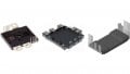
Another highly-integrated example is the HiperLCS™ IC, an integrated LLC power stage with a multi-function controller, high-side and low-side gate drivers, and two power MOSFETs in a half-bridge configuration. Devices like these can eliminate dozens of external components in a circuit, reduce assembly cost, and dramatically shrink magnetics size while using SMD ceramic output capacitors.

Figure 1: HiperLCS showing very low component count
Reducing the BOM
This reduction in external power components is a significant force multiplier in a system. As another example, Power Integration’s HiperTFS™-2 devices bring a high-power two-switch-forward converter and a mid-power flyback (standby) converter into a single, low-profile eSIP™ power package. This single-chip solution provides the controllers for both of the two-switch-forward and flyback converters, high- and low-side drivers, all three of the high-voltage power MOSFETs while eliminating the converter’s need for costly external pulse transformers.
The device is ideal for high power applications that require both a main power converter (two-switch forward) up to 586 W peak, and a standby converter (flyback) up to 20 W. The devices operate over a wide input voltage range, and can be used following a power-factor correction stage such as HiperPFS™-4, and has a self-biased high-side driver eliminating the bias winding and drive circuitry normally required. It is important to note that the solution addresses the system needs for high efficiency and high reliability, -but does not compromise performance for the sake of reduced parts count.

Figure 2: Highly integrated two-switch-forward plus flyback power conversion
High device integration allows for a smaller form factor, with delivering benefits throughout the system beyond higher power density and reduced component count by incorporating control, gate drivers, and power MOSFETs.
Enhancing performance
The HiperPFS-3 family of devices take that integration even further by incorporating a continuous conduction mode (CCM) boost PFC controller, gate driver, ultra-low reverse recovery diode, and high-voltage power MOSFET into a compact, heat-sinkable package. In addition, the HiperPFS-3 family features a light-load digital enhancer that increases the power factor to more than 0.92 at 20% load (highline) plus an efficient "light load" mode which consumes less than 60 mW in no-load.

Figure 3: HiperPFS-3 – Note the integrated CCM-boost diode and simplified feedback network feeding the integrated non-linear amplifier via the FB pin
The HiperPFS-3 families' variable-frequency continuous-conduction mode operation minimizes loss by maintaining a low average switching frequency and by modulating that frequency across each input half-cycle, also suppressing peak EMI. Systems using HiperPFS-3 typically minimize the total X and Y capacitance requirements of the converter and the inductance of both the boost choke and EMI noise suppression chokes, thereby reducing overall system size and cost.
HiperPFS-4 devices use the same innovative control technique that eliminates the need for external current-sense resistors and their associated power loss, and also adjusts the switching frequency over output load, input line voltage, and across the input line cycle. This maximizes efficiency, particularly at light loads, and minimizes the EMI filtering requirements due to its wide-bandwidth spread-spectrum effect. The devices use digital line monitoring, line feed-forward scaling, and power factor plus THD enhancement at light load, while using analog techniques for the core controller in order to maintain extremely low no-load power consumption.
HiperPFS devices also feature an integrated non-linear error amplifier for enhanced load transient response, a user-programmable Power Good (PG) signal as well as user-selectable power limit functionality. Protection features include UV, OV, brown-in/out, and hysteretic thermal shutdown, as well as cycle-by-cycle current limit and Safe Operating Area (SOA) protection of the power MOSFET, output power limiting for overload protection, and pin-to-pin, short-circuit protection.
Efficiency without PFC
The DER-447 reference design creates a high-efficiency system without PFC. The 184 W constant voltage and current power supply uses the HiperLCS LCS705HG and the LinkSwitch™-TN LNK302D. The solution can accept from 90 VAC to 132 VAC and deliver 184 W (23 V at 0.5 to 8 A). To highly integrated LLC stage further reduces parts count. The LNK302D is used in a flyback mode as a bias supply to provides power for both primary and secondary control circuitry. The secondary control circuitry provides a CV/CC output characteristic for use in battery charging applications.

Figure 4: CV CC output characteristic of DER-447 showing excellent stability across line
The DER-580 is a 118 W flyback design taking from 180 VAC to 264 VAC and delivering 59 V at 2.0 A for battery charging applications. The high-power flyback design also has a low component count, and offers features like 66 kHz operation for high efficiency (>90% at 230 VAC). At charging currents below ~0.5 A, the output voltage switches form the 59 V charging voltage to a float voltage of 56 V to maintain battery charge without overcharging.

Figure 5: CV CC output characteristic of DER-580 showing the light load voltage step to ensure support of both charging and float-voltage modes depending on charge-state
Based on TOPSwitch TOP267EG with no PFC input stage, it is designed to operate without a fan, and includes a thermal switch that reduces the current limit at elevated temperature (thermal foldback) to enable continued charging at reduced output current without thermal shutdown. Solutions like these maximize function without reducing safety or reliability of the system while still providing the service desired.
Driving ahead
Creating power systems for the next generation of advanced vehicles using battery systems must address the increased demands for size, power density, reliability, and performance. Using highly-integrated building blocks and designs intended to maximize the benefits of each component in the system will go a long way to addressing those concerns.
About the Author
Chris Lee works as a Product Marketing Manager at Power Integrations. He is responsible for driving business growth for applications including computing, server, high power battery chargers for power tools, e-Bikes, e-Scooters, display, and general consumer applications. He is also the product owner of LLC, PFC, Flyback, and Two-Switch Forward product lines. He is particularly skilled in semiconductors, product marketing, and power management as well. He earned his Bachelor's Degree in Electrical Engineering at the University of Califonia, Davis.
Alix Paultre works as an Industry Commentator. He is particularly skilled in publishing, publications, and digital media. He earned his Bachelor of Arts in English at the Community College of the US Army.
This article originally appeared in the Bodo’s Power Systems magazine.