Facebook
 Google
 GitHub
 Linkedin
Reaching New Efficiency Heights with 3-Level DC-DC Converters
Learn how 3-Level DC-DC converters boost efficiency and power density in high-power electronics by lowering voltage stress, cutting switching losses, and reducing heat.
As consumer and industrial electronics push toward higher power delivery in smaller footprints, designers face an increasingly difficult challenge: achieving high efficiency without overheating or sacrificing reliability. This challenge is particularly acute in applications like USB Power Delivery Extended Power Range (USB-PD EPR) adapters, docking stations, and high-performance computing equipment, where compact enclosures must handle sustained high power levels.
Traditional two-level DC-DC converters, while proven and widely adopted, are hitting a performance ceiling in these scenarios. Switching losses, voltage stress on components, and thermal constraints have become limiting factors. The 3-Level DC-DC converter architecture offers a path forward, delivering significant improvements in efficiency, thermal headroom, and power density.
How the 3-Level DC-DC Converter Works
A 3-Level DC-DC converter introduces an intermediate switching node between the input voltage and ground. Instead of swinging a switch node across the full input voltage, the topology splits the voltage in half during each switching cycle using a pair of capacitors (often called a flying capacitor arrangement).
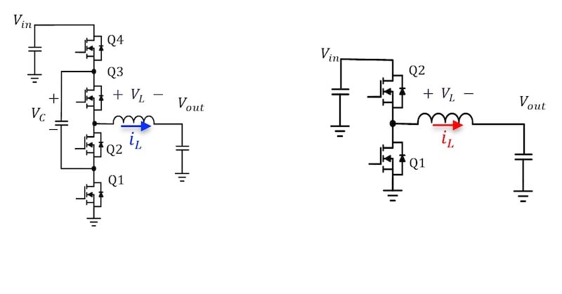
Figure 1. 3 level vs 2 level DC-DC convertor topologies
Key benefits include:
- Reduced Voltage Swing per Switch—Each MOSFET sees only half of the input voltage, lowering switching loss and enabling the use of lower-voltage, lower-RDS(on) MOSFETs.
- Lower Voltage Stress on Components—Capacitors, MOSFETs, and magnetics can be selected from higher-performance, lower-voltage product families.
- Reduced Switching Losses—The energy lost per transition, proportional to V², is greatly reduced.
Efficiency Advantages
In high-voltage step-down scenarios, 3-Level converters routinely achieve efficiencies exceeding 98%. For example, in a 48 V to 20 V USB-PD EPR stage, switching losses can be reduced by over 40% compared to a two-level design.
Thermal Benefits:
- Lower loss means less heat per watt delivered.
- Designers can reduce heatsinking or push for higher power density without breaching thermal limits.
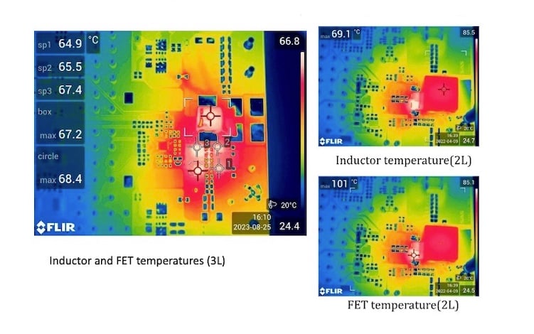
Figure 2. Thermal performance comparison of 3-Level and 2-Level DC-DC converters
Efficiency and Thermal Calculations Example
To illustrate the efficiency and thermal advantages of the 3-Level DC-DC topology, consider a 48 V to 20 V, 240 W USB-PD EPR stage operating at 300 kHz. The following calculations use realistic but illustrative MOSFET parameters for two-level and three-level buck converters.
Assumptions:
- Vin = 48 V, Vout = 20 V, Iout = 12 A, fs = 300 kHz
- Two-level: tr/tf = 15 ns, Coss_total = 400 pF, Qg = 18 nC, Rds(on) = 10 mΩ (per FET)
- Three-level: tr/tf = 12 ns, Coss_total = 600 pF, Qg = 12 nC, Rds(on) = 6 mΩ (per FET, two in series per path)
- Fixed losses (controller etc.) = 0.25 W
|
Metric |
Two-level |
Three-level |
|
Inductor copper loss (W) |
1.35 |
0.654 |
|
Inductor core loss (W) |
0.8531 |
0.321 |
|
FET switching overlap (W) |
2.592 |
1.182 |
|
FET Coss loss (W) |
0.238 |
0.152 |
|
FET gate-drive (W) |
0.21 |
0.21 |
|
FET conduction (W) |
1.84 |
1.864 |
|
Power-stage subtotal (W) |
7.0831 |
4.383 |
|
Fixed (controller etc.) |
0.25 |
0.25 |
|
Total loss (W) |
7.3331 |
4.633 |
|
Output power (W) |
240 |
240 |
|
End-to-end efficiency (%) |
96.9% |
98.1% |
Switching-related losses (P_sw + P_coss + P_gate) drop from 3.04 W in the two-level case to 1.54 W in the three-level case. Inductor loss drops from 2.2W to 0.98W. End-to-end efficiency improves from 96.9% to 98.1% for the same 240 W output power.
Thermally, the reduced loss per MOSFET translates to significantly lower junction temperature rise. In this example, the hottest MOSFET in a two-level design might experience a +76 °C rise above ambient, while in the three-level design, individual device dissipation drops to ~0.85 W, resulting in only a +42 °C rise for similar cooling conditions.
Real-World Application Examples
The benefits of 3-Level converters are most apparent in compact, high-power applications where every watt and every cubic centimeter count. In USB-PD Extended Power Range (EPR) adapters delivering 140 W–240 W, the reduced ripple current and lower device stress enable slimmer inductor designs, translating directly into smaller, lighter chargers that run cooler in the user’s hand.
Docking stations and monitors with integrated USB-C power delivery also benefit, as the reduced thermal footprint allows designers to integrate multiple high-speed data ports without resorting to bulky heat sinks. In high-performance computing environments—such as servers, AI accelerators, and edge devices—the 3-Level architecture achieves efficiencies above 98%, minimizing cooling overhead while maintaining reliability under continuous load.
Even industrial and medical instruments with long duty cycles gain from smaller magnetics and higher efficiency, extending system lifetime and lowering energy cost. These examples highlight how 3-Level topologies move beyond theory to deliver tangible advantages across diverse markets.
Next Leap in Power Delivery Performance
The 3-Level DC-DC converter is not just an incremental improvement—it’s a significant architectural step toward meeting the power density, efficiency, and thermal demands of next-generation electronics. By halving voltage stress and cutting switching losses, this topology opens the door to over 98% efficiency, reduced component temperatures, and higher reliability.
For engineers designing in the era of USB-PD EPR and beyond, adopting 3-Level architectures may well be the key to unlocking the next leap in power delivery performance.
All images used courtesy of Renesas.