Facebook
 Google
 GitHub
 Linkedin
Soldering Materials for the Next Generation of Power Electronics
This article highlights Tamura Corporation new soldering materials development for jointing technology in response to the requirement of power electronics.
The jointing technology required for advanced power electronics requires achieving high reliability, heat resistance etc. Tamura Corporation, a global company in the field of electric and electronic technology, has developed a new jointing material as a response to these requirements.
Introduction
Tamura Corporation is a global company that contributes to the electronics industry through information equipment, electronic components, electronic chemicals, and factory automation systems. As measures against global environmental problems, it is becoming more important to electrify vehicles and to secure electricity through renewable energy. Under such circumstances, power electronics, which contribute to the efficient use of electric energy (generation, transportation, consumption, etc.) is more important than ever. In power electronics, power devices and power modules used for a wide operating voltage ranging from hundreds of volts to hundreds of thousands of volts are the main components responsible for power conversion and control. High reliability is also required for power devices and power modules.
In this report, the bonding technology developed for the power electronics based on the high level jointing technology from Tamura Corporation cultivated in automotive market is introduced.
Reports about Tamura’s soldering materials for power electronics
According to [1] solder composition, [2] flux type, and [3] product form, the outline of the solder material for power electronics developed by Tamura Corporation is summarized in Figure 1.

Figure 1: Tamura’s Soldering Technology for die attach and substrate attach
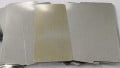
Three types of solder composition are prepared as follows. (1) SAC305 which is standard as the lead free solder. (2) Modified SAC which improves the operating temperature up to 150°C and 175°C while setting the mounting workability to the same level as SAC305. (3) TLPS with a melting temperature of 300°C (despite heat treatment is taken place at 240°C). As the flux for power electronics, we provide two types of flux (1) a residue free type and (2) an anti-cracking type. These fluxes are applied as solder paste with solder of SAC305. In order to achieve voidless for die attachment which requires high reliability, TLPS’s product form is a film type.
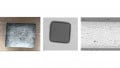
A solder paste of residue free type (D131-204-199-33) and a conventional type is applied on the electrode pad of PWB, and the appearance after the reflow process is shown in Figure 2. In the conventional type on the right side, there is flux residue on the solder surface after reflow, so there is a glossy feeling due to the flux residue resin.

Figure 2: Appearance of flux residue for D131-204-199-33(flux residue free type) and conventional type
On the other hand, the residue free type (D131-204-199-33) shows metallic luster of the solder itself resulted from no flux coating on the solder. This is because the residue free type flux ingredients are designed to evaporate by the heat in reflow oven at the portion not in contact with the solder. As a result, in case of bonding of die attachment, substrate, etc., the flux protruding outside the junction element evaporates in the reflow process and the flux cleaning process can be omitted.
Solder joint of 3216 chip resistors are formed on the PCB with SAC 305 alloy and Modified SAC alloy respectively. 3,000 cycles of heat cycle test is carried out at a temperature range of -40°C to 150°C. After every 1,000 cycles, solder crack in solder fillet portion on the side of the chip is observed. Figure 3 shows the results of observing the crack progress rate generated by the solder of SAC 305 and Modified SAC in each 1,000 cycles. As Figure 3 shows, durability of Modified SAC (# 287) is about 3 times higher than SAC 305 in the heat cycle test (3,000cycles@ -40°C to 150°C). Modified SAC has been improved in terms of mechanical strength and creep characteristic peculiar to solder. In addition, the suppression of enlargement of solder structure and growth of intermetallic compound at electrode interface has been taken place. Currently, we are developing a more robust solder material which can withstand heat cycle test of -40°C to 175°C.
Tamura Corporation has been developing bonding materials specialized for die attachment for Wide-Band-Gap semiconductors such as Silicon Carbide which are expected to be used at the higher junction temperatures than Silicon. Since it is assumed that the junction temperature of Silicon Carbide is about 250°C, melting temperature of solder needs to be more than 300°C for the die attachment. Recently, the sintered silver material with the silver nanoparticles is a promising candidate as the die attachment.

Figure 3: Comparison of crack resistance between Modified SAC(#287) and SAC305
This is mainly because this material can be bonded at temperature as low as about 250°C, although its melting temperature is about 900°C. However, in order to densely sinter the nanoparticle of silver, it is necessary to apply pressure on it during heating, and this is a problem for mass production in the field of high volume market such as automotive. Therefore, Tamura Corporation has designed and been developing new soldering material which achieves bonding with no pressure at the same reflow temperature(240°C) as SAC 305 and the melting temperature of solder material exceeds 300°C after soldering reflow treatment. The die attachment plays a role of quickly releasing heat from a semiconductor operating at high temperature. At this time, voids in the die attachment lead to the unevenness of heat flow (so called Hot spots occurred). As the results the bonding reliability is remarkably deteriorated. For this reason, it is required to form a void-free joint in the die attachment. In order to achieve void free, Tamura’s TLPS has been designed in a film of preformed solder.

Figure 4: DSC curve and cross section of Tamura’s TLPS before heating (a) and after heating (b)
A cross section of the film composed of low melting point solder and copper powder is shown in Figure 4 (a). Copper (black area) and solder (white area) are uniformly formed, and voids are not observed in it. When thermally analyzing the TLPS before heat treatment, an endothermic DSC peak derived from the low melting point solder shown in Figure 4 (a) is observed on the left side of the DSC curve. On the other hand, when the solder composition obtained by heat treatment at 240°C is thermally analyzed, there is almost no endothermic DSC peak in the temperature range of 400°C as shown in Figure 4 (b).
It is considered that the melting point of the obtained solder compound exceeds 400°C. By applying Tamura’s original flux to the surface of the TLPS, solder joint is formed upon the heat treatment at 240°C. A cross section of the solder composition after heat treatment at 240°C is shown in Figure 4 (b). No voids and no peeling at the interface with the copper plate are observed. In the cross-sectional structure of TLPS obtained after heating, it is found that a solder (white area) is formed on the network structure and IMC (intermetallic compound: gray area) surrounds copper (black area). In this experiment, a pressure of 0.6 MPa was applied during heating.
Summary
Hereby we reported new soldering materials, which are developed with our original technologies, for power electronics. From now on, Tamura will develop a die attachment that is highly reliable and excellent in workability, aiming at bonding without pressure which the market and technology trend desire now and future.
Remark
s#1: Modified SAC is a SAC305 containing additional elements; Operating temp. 175°C type is under development; Operating temp. 150°C type is on the market
#2: TLPS means transient liquid phase soldering Our TLPS film is under development
#3: Under development
#4: #287 is a solder alloy composition developed by Tamura Corporation