Facebook
 Google
 GitHub
 Linkedin
Utilizing GaN Inverters for Battery-Powered Motor Drive Applications
GaN transistors and ICs increase power density in motor drive applications. An optimal lay-out approach allows obtaining ring-free output switching waveforms and clean current reconstruction signals either from leg shunts or from in-phase shunts.
Many applications such as warehouse autonomous robots and lean production lines collaborative robots require that inverters for each motor have high power capability while being compact and light. This poses a challenge to designers because power, size and weight have always been opposing attributes. In battery-powered applications, every cubic inch of occupied space and every gram of weight saved allow longer operation time between two battery charges. GaN FETs from Efficient Power Conversion help designers in increasing the power density to win the challenge.
EPC9145 Motor Drive Power Evaluation Board
The EPC2206 80 V 2.2 mΩ eGaN® FET (Figure 1) is an optimum candidate for applications where the Bus voltage is below 70 VDC. In motor drives, PWM frequency is usually kept below 50 kHz and dead times are above 500 nanoseconds. In these cases, the switch RDSON is the primary parameter that designers look at. The thermal capability, in particular, the device junction to case thermal resistance, Rθjc, is the second parameter to be considered. Conventional MOS-based solutions have one, or many devices in parallel per each switch and are based either on 5 x 6 mm or 10 x 10 mm packages, as shown to scale in Figure 1.

Figure 1. EPC2206 80V 2.2mohm GaNFET (on the left) compared to similar RDSON MOSFETs. Picture in scale.

Figure 2. EPC9145 - 3 phase inverter power board based on EPC2206 – 10 x 12 cm
EPC9145 is a motor drive evaluation board that features the EPC2206 and has everything needed except the microcontroller to drive a motor on the board. It can be operated with a maximum bus voltage of 70 VDC, and a maximum phase current of 25 ARMS. The motor controller can be chosen from those available on the market and can be connected using the proper EPC mate board. In Figure 2, from the left to the right there are the control connector, the signal conditioning circuit for voltages and currents feedback to the external microcontroller, the ceramic capacitor bank, three phase inverter with leg shunts and phase shunts and, finally, the motor connector.
dv/dt Switching Waveforms
The EPC9145 PCB has been laid out following the EPC optimal layout rules (Figure 4), that guarantee the lowest inductance in the power loop. The main criterion is to observe symmetry in the component placement, and to constrain the entire high frequency path in the top and first inner layer. In EPC9145 case, layout is slightly more complex because there are leg shunts in the high frequency power loop as shown in Figure 3.

Figure 3. Detailed view of the switching cell

Figure 4. EPC optimal layout recommendation
The HF capacitors are nine 220 nF size 0603, all in parallel, to reduce the overall inductance at high frequency. The same principle applies for the 1mΩ leg shunt sensor, which is made with four SMD resistors 4 mΩ 0805 wide body. The result is visible in Figure 5 where the switching node of phase V swings over time in both rising and falling edges as shown.
The pictures in Figure 5 have been obtained with infinite persistence to capture all waveforms, so that the maximum dv/dt is clearly visible. No voltage overshoot has been observed and the dv/dt is clearly in range used in typical motor drive applications. The careful reader can observe that the dead time was set to 50 ns (2.5 divisions).

Figure 5. Phase V rising edges at 30V bus / Phase V falling edges at 30V bus
Current Sensing In-Phase vs. Leg Shunts
When using discrete eGaN FETs or a GaN ePowerTM stage IC in an inverter for motor drive, it is common to use an in-phase current shunt together with an isolated (functionally or galvanically) IC that extracts the low voltage differential signal across the shunt resistor from the common mode of the switching phase. This approach has the advantage of giving the user continuous access to the phase current signal across the entire PWM period, except during switching events, where the signal may be influenced by the phases dv/ dt. However, when compared to leg shunt sensing, the higher cost and lower bandwidth of the in-phase shunt solution may be detrimental for GaN inverter adoption in motor drives.

Figure 6. In-phase and leg shunt current sensing comparison – NOTE: noise in the picture is picked up by nonoptimal measuring setup. Real signals are cleaner as it can be shown by controller current reconstruction.
The EPC9145 offers the user the chance to test both solutions and decide which fits best in his application. In fact, there are in-phase 1 mΩ shunts as well as 1 mΩ leg shunts per each switching cell. The 20x amplification gain, offset and polarity are the same for both circuits so that the user can connect either the one or the other sensing scheme to the external microcontroller without making any firmware change. As shown in Figure 5, the insertion of the shunt in the low side leg does not have detrimental effect on the switching behavior.

Figure 7a. Inner layer with shunt signal kelvin connections

Figure 7b. Layers above and below with analog ground shielding of shunt kelvin traces
A comparison of the two current measuring methods, as well as the signal obtained from a current probe connected at the output of the inverter, is shown in Figure 6. When phase voltage is high, the signal across the leg shunt is null and the output of the amplifier is centered at 1.65 V; when phase voltage is low, the current which is flowing in the in-phase shunt is also flowing in the leg shunt so the two amplified signals overlap. Conventional field-oriented control algorithms measure the current in the middle of the phase low voltage pulse (indicated by two stars in Figure 6), so, by simply changing the position of three jumpers on the EPC9145 board, it is possible to use any of the two signals.
Layout Rules for Accurate Current Sensing
The EPC9145 demonstrates the good practice in routing low voltage signals from the shunt resistors across the power board to the point where they are amplified and brought to the microcontroller connector. The main criterion is to perform kelvin measurement across the shunt and bring the traces as close as possible and shielded by analog ground cages on layers above and below the routing layer as shown in Figure 7. Another good practice is to divide digital and power ground from analog ground and connect them together in one single point far from the power loop paths.

Figure 8. 40 kHz 50 ns DT operation, 60 VDC 17.5 ARMS phase current – leg shunt measure

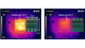
Figure 9. Infrared picture (confirmed by a thermocoupler) at 60 VDC 10 ARMS phase current 40 kHz 50 ns DT
Operation Without Heatsink
Both in-phase and leg sensing were used when testing the EPC9145 in a motor bench setup with a hysteresis brake. Current and voltage waveforms at 17.5 ARMS 60 VDC are shown in Figure 8. Figure 9 shows the temperature across the EPC2206 without heatsink and no air convection. In this case the current is 10 ARMS at 60 VDC and the difference vs. ambient temperature is 30°C. Tests with heatsink with and without air convection are on-going and results will be reported soon in the board quick start guide.
The benefit of 100 kHz Operation
An eGaN-based inverter can be easily operated at 100 kHz. The advantage is that the input voltage and current ripple decrease when the PWM frequency is increased, allowing the user to remove the electrolytic capacitors and use only ceramic that are smaller, lighter, and more reliable. The EPC9145 is populated on the top surface with ceramic capacitors and on bottom with electrolytic capacitors. There are placeholders on both top and bottom layers so the user can mount, or un-mount the capacitors and make their own trials and judgements to find the right operating point that optimizes weight, size, and thermal operation.
Conclusions
Many battery-powered motor applications are moving from conventional Si MOSFET, low PWM frequency to GaN inverters that can run at higher PWM frequency and bring the advantage of reducing the size and the weight without sacrificing the overall system efficiency. With proper gate driving and optimal layout, the switching waveforms are clean and dv/dt is easily managed.
References
[1] A.Lidow, M. De Rooij, J. Strydom, D. Reusch, J. Glaser, “GaN Transistors for Efficient Power Conversion.” Third Edition, Wiley. ISBN 978-1-119-59414-7
[2] D.Reusch, Fred C. Lee, David Gilham, Yipeng Su, “Optimization of a High Density Gallium Nitride based Non-Isolated Point of Load Module”, ECCE 2012 Raleigh, NC
[3] M. Vujacic, M. Hammami, M. Srndovic, G. Grandi, "Analysis of dc-Link Voltage Switching Ripple in Three-Phase PWM Inverters," Energies. 2018; 11(2):471. https://doi.org/10.3390/ en11020471.
[4] M. Palma, “GaN ePower Stage IC-Based Inverter for BatteryPowered Motor Drives Applications”, Bodo’s Power April 2021