Facebook
 Google
 GitHub
 Linkedin
The Interleaved Inverting Charge Pump - Part 2: Implementation and Results
In Part 1 of this series, we introduced a unique method of generating a low noise negative rail from a positive supply, and we presented a derivation of the equations governing its operation. Part 2 dives into a practical example of this interleaved inverting charge pump (IICP) implementation with Analog Devices’ ADP5600.
We compare the voltage ripple and radiated emissions of the ADP5600 to a standard inverting charge pump to show how interleaving improves low noise performance. We also use the equations from Part 1 to optimize the performance of this solution in the context of applying it in a low noise phased array beamforming circuit.
Commercially Available Interleaved Inverting Charge Pump
As stated in Part 1, IICPs are used within integrated circuits to generate small negative bias rails. The ADP5600 uniquely combines a low noise IICP with other low noise features and advanced fault protection. The ADP5600 is an interleaved charge pump inverter with an integrated low dropout (LDO) linear regulator. Its unique charge pump stage exhibits reduced output voltage ripple and reflected input current noise when compared to conventional inductive or capacitive based solutions. Interleaving is clever as a low noise concept, but interleaving channels is not a cure-all for noise problems. Achieving true low noise requires an IC specifically designed to realize the low noise advantages of an IICP, while keeping the solution size small and efficient.
Fixed and Programmable Switching Frequency
Many inverting charge pumps operate to a few hundred kHz. This relatively low frequency limit necessitates relatively large capacitors and limits where the frequency spurs can be placed. The ADP5600 can operate at a switching frequency from 100 kHz to 1.1 MHz, allowing it to be used effectively in modern systems. Furthermore, this frequency is always fixed—there is no frequency variation vs. output load. Switching frequency variation (spread spectrum frequency modulation) is commonly implemented to improve the charge pump’s efficiency, but it may create problems in noise sensitive systems.

Figure 1. ADP5600 interleaved inverting charge pump simplified block diagram. Image used courtesy of Bodo’s Power Systems
External Frequency Synchronization
Many low noise systems need to place high amplitude switching noise into defined frequency bands where the generated noise minimally impacts the system. With this in mind, converters’ operating frequencies are synchronized in noise-sensitive systems, but synchronization is a rare feature in charge pump inverters. In contrast, the ADP5600 can be synchronized to an external clock up to 2.2 MHz.

Figure 2. ADP5600 interleaved inverting charge pump test setup. Image used courtesy of Bodo’s Power Systems
Low Dropout Voltage Regular
Because the ADP5600 covers a wide input voltage range, its charge pump output voltage may be too high to power lower voltage circuitry. Therefore, the ADP5600 includes an LDO post regulator. It also features a positive voltage referenced power-good pin for easy power sequencing when the LDO output is in regulation.
Fault Protection
Finally, the ADP5600 includes a comprehensive set of fault protection features for robust applications. This includes overload protection, shorted flying capacitor protection, under-voltage lockout (UVLO), precision enable, and thermal shutdown. An additional novel feature, flying capacitor current limiting, also reduces the peak current spikes when charging the flying caps.
Test Data from the ADP5600
Part 1 presented theoretical proof that IICP architecture significantly improves ripple when compared to non-interleaved solutions. For the sake of brevity, the derivations shown in Part 1 were ideal—they overlooked parasitics, layout dependencies (IC and PCB), timing mismatches (that is, an imperfect 50% oscillator), and RDS mismatches. These factors result in some deviation from the calculated and measured voltage ripples. As always, it is best to put the ADP5600 into action, observe its performance, and use the derived equations to guide the optimization of the circuit for the best performance.
A standard ADP5600 evaluation board was used here, but with the insertion of RFLY, and modifications to the values of CFLY and COUT. Furthermore, we use the ADP5600’s SYNC feature to vary the switching frequency. The block diagram in figure 1 shows that the individual charge pumps switch at one-half of this SYNC frequency; that is, fOSC = ½ fSYNC.
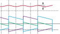
Figure 3 and figure 4 show the output voltage ripple for the interleaved and non-interleaved inverting charge pump, respectively, when operated under the same conditions.
With these conditions, the input and output voltage ripples of the ADP5600 are nearly 14 times lower than a traditional inverting charge pump. We can also determine if this voltage ripple matches the equations derived in Part 1 of this series. Recall from Part 1 that the output (or input) voltage ripple of an IICP was given by:
\[\Delta V_{OUT}=\frac{I_{LOAD}}{4\times f_{OSC}\times C_{OUT}}-I_{LOAD}\times(R_{OUT}-2\times R_{ON})\times\frac{C_{FLY}}{C_{OUT}}\times\frac{\beta-1}{\sqrt{\beta}}\,where\,\beta+e=e^{1/8fRC}\]
Equation 1.
\(where\,f\,is\,f_{OSC},\,R\,is\,R_{ON},\,and\,C\,is\,C_{FLY}\).
Using equation 1, and substituting in real values for ROUT and RON, it is possible to compare the calculated and measured output voltage ripple. Table 1 gives these results for a variety of tested configurations and notes the improvement over a non-interleaved charge pump implementation.
Table 1 shows that the interleaved voltage ripple closely matches the prediction from equation 1. The improvement over the standard, non-interleaved, inverting charge pump is also shown. Some setups within this table also include an additional external resistance, RFLY, connected in series with CFLY. Those results demonstrate that RFLY further reduces the voltage ripple, but at the expense of charge pump output resistance. This was also predicted by equation 1 and the analysis from Part 1 of this series.
In addition to the output voltage ripple, the radiated emissions from the IICP also show improvement over a standard charge pump. To measure this, a 25 mm antenna was placed over the evaluation board (Figure 5) and various configurations were tested. Figure 6 shows a comparison of one such configuration vs. a standard non-interleaved charge pump inverter. The IICP topology results in a 12 dB to 15 dB reduction in noise for the first and third switching harmonics.
| fOSC (kHz) | COUT (μF) | CFLY (μF) | RFLY (Ω) | Measured VOUT (V) | Measured ROUT (Ω) | VOUT Ripple (mV) |
Improvement over Noninter leaved |
|
| Meas | Calc | |||||||
| 250 | 1.6 | 1.6 | 0 | 11.48 | 10 | 5.3 | 6.0 | 12× |
| 250 | 1.8 | 1.8 | 25 | 8.86 | 63 | 3.4 | 3.2 | 18× |
| 250 | 4.6 | 1.6 | 0 | 11.48 | 10 | 1.9 | 2.4 | 12× |
| 500 | 2.8 | 1.6 | 0 | 11.45 | 11 | 2.5 | 2.9 | 7.5× |
| 500 | 1.8 | 1.8 | 25 | 8.74 | 65 | 3.1 | 2.7 | 10× |
| 1000 | 1.6 | 1.6 | 0 | 11.40 | 12 | 4.3 | 4.2 | 3.7× |
| 1000 | 1.8 | 1.8 | 25 | 8.438 | 71 | 2.8 | 2.8 | 5.6× |
Table 1. VOUT Ripple for Various Use Cases; VIN = 12 V, ILOAD = 50 mA, RON = 2.35 Ω. The actual capacitances of COUT and CFLY (with their capacitive derating at voltage) were used, not their nominal values.

Figure 3. ADP5600 IICP output voltage with VIN = 6 V, COUT = CFLY = 2.2 μF, fOSC = 250 kHz, ILOAD = 50 mA. Image used courtesy of Bodo’s Power Systems

Figure 4. Standard inverting charge pump output voltage with VIN = 6 V, COUT = CFLY = 2.2 μF, fOSC = 250 kHz, ILOAD = 50 mA. Image used courtesy of Bodo’s Power Systems

Figure 5. Radiated emissions test setup with the ADP5600 evaluation board. Image used courtesy of Bodo’s Power Systems
Application Example of the IICP
Low noise power is required for data converters, RF amplifiers, and RF switches. The main challenges facing power supply designs in these systems are:
- Power dissipation and high-temperature operation
- EMI immunity and low EMI contribution
- Large input voltage ranges
- Minimizing solution size and footprint
To illustrate the complete design and advantages of the IICP, let us consider an application that powers RF amplifiers, RF switches, and phased array beamformers. The application is included in the ADTR1107 datasheet and replicated in Figure 7.
In this example, several high power positive voltage rails are required—which are left here as a job for inductive buck converters. Two negative rails are also needed: AVDD1 and VSS_SW. AVDD1 is used by the ADAR1000 to generate low noise bias rails for VGG_PA and LNA_BIAS. AVDD1 is –5 V at 50 mA, and VSS_SW is the –3.3 V at <100 μA rail to the RF switch within the ADTR1107. Four ADTR1107s are used per ADAR1000, so the –3.3 V rail draws a max of 1 mA. Typically, the supply rail into these systems is 12 V.
The ADP5600 is a good choice to produce –5 V at 50 mA and –3.3 V at 1 mA rails from 12 V, as it achieves low input and output voltage ripple, and low radiated emissions. Furthermore, the ability to synchronize the switching frequency over a wide range allows the switching noise to be placed where it will have the least impact on the system. Figure 8 shows the final design.

Figure 6. Radiated emissions, VIN = 12 V, ILOAD = 50 mA, CFLY = COUT = 2.2 μF, fSYNC = 500 kHz. Green = standard, blue = IICP. Image used courtesy of Bodo’s Power Systems

Figure 7. ADAR1000 plus four ADTR1107 power rails. Image used courtesy of Bodo’s Power Systems

Figure 8. ADP5600 and LT3093 are used to power AVDD1 and VSS_SW. Image used courtesy of Bodo’s Power Systems
The LT3093 is a very low noise LDO linear regulator, which is capable of high voltage that allows the ADP5600 charge pump output (CPOUT) to be connected directly to its input. Its –5 V output is set by the resistor on the SET pin, and a programmable power-good pin can notify other systems when the AVDD1 rails are in compliance. The ADP5600’s LDO regulates the much lower current VSS_SW rail. While not as low noise, or as high of a power supply rejection ration (PSRR) as the LT3093, it is capable of providing a stable rail for VSS_SW. The output voltage ripple of all three rails (charge pump, AVDD1, and VSS_SW) is shown in Figure 9.

Figure 9. Charge pump output voltage ripple for VIN = 12 V, COUT = 10 μF (nominal), CFLY = 2.2 μF (nominal), fSYNC = 1 MHz (fOSC = 500 kHz), ILOAD = 50 mA. Image used courtesy of Bodo’s Power Systems
Conclusion
This two-part series presented a new method to generate low noise negative rails from a positive supply. Part 1 covered the concepts behind interleaved inverting charge pump operation. Part 2 put these ideas into practice with a complete solution built and tested using Analog Devices’ new ADP5600. This solution was optimized with the mathematical model derived in Part 1. The conducted and radiated emissions were compared to a standard inverting charge pump. Under some conditions, an 18-fold improvement was realized over standard charge pump inverters, which is important for meeting the low noise requirements of modern precision and RF systems.
Acknowledgments
With gratitude for the assistance of Sherlyn Dela Cruz, Roger Peppiette, and Steve Knoth.
About the Authors

Image used courtesy of Bodo’s Power Systems
Jon Kraft is a senior staff FAE in Colorado and has been with ADI for 13 years. His focus is software-defined radio and aerospace phased array radar. He received his B.S.E.E. from Rose-Hulman and his M.S.E.E. from Arizona State University. He has nine patents issued (six with ADI), and one currently pending.

Image used courtesy of Bodo’s Power Systems
Alexander Ilustrisimo graduated from Central Philippine University with a bachelor’s degree in electronics engineering. He joined ADI in 2014 and has worked as an applications engineer for power management products for more than six years, with a focus on LDO regulators and switching regulators.
This article originally appeared in Bodo’s Power Systems magazine.
Related Content