Facebook
 Google
 GitHub
 Linkedin
The Expanding Markets for GaN Technology
This article discusses the expanding markets for GaN technology and offers some insights and reasons why it is better than their silicon-counterparts.
Key Take Aways
- GaN technology is in its infancy and will follow a “Moore’s Law” path of improvement by doubling performance every two years.
- Integrating power devices on a single chip is straightforward in GaN and improves cost and performance significantly. Beyond today’s $12B power transistor market is the $31.2B power management market. GaN technology is poised to attack these applications with superior cost and performance by integrating analog and power functions onto a single semiconductor chip.
- The entire $300B semiconductor industry, now dominated by silicon, is a “bull’s-eye” target for GaN technology.
In the past five issues of Technology Driving Markets we traced a path from the basic properties of a gallium nitride crystal, to the electrical characteristics that result, to how this material, when transformed into an eGaN® FET, can enable some amazing new end-use applications, such as wireless power transfer, LiDAR, and envelope tracking. eGaN FETs can also replace the aging silicon-based power MOSFET in most existing applications including AC-DC and DC-DC power conversion, yielding substantial performance gains. The prize is a $12B market now occupied by an aging incumbent.
The Expanding Markets for GaN Technology
The GaN technology journey is just beginning, and we are still far from its theoretical performance limits. It is quite reasonable to expect a rate of improvement reminiscent of Moore’s Law, which predicted the growth of microprocessor technology – doubling of product performance every two to four years for at least the next decade. (see figure 1)
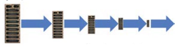
Figure 1: Moore’s Law for eGaN FETs
Beyond just performance and cost improvement, the greatest opportunity for GaN technology to impact the power conversion market comes from its intrinsic ability to integrate both power-level and signal-level devices on the same substrate. GaN technology, as opposed to common silicon IC technology, allows designers to implement monolithic power systems on a single chip in a more straightforward and cost-effective way.
Today, eGaN FETs are made such that the product is a single discrete transistor. These devices work in conjunction with driver and control integrated circuits. Transistors of all types, plus their accompanying integrated circuits, form the majority of the power management market. According to IHS iSuppli Research, in 2011 this market in total was $31.2B.
Is GaN a good candidate to replace this entire $31.2B market? We believe the answer is yes, and that it will occur in stages over the next few years.
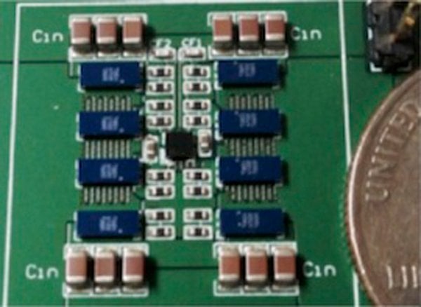
Figure 2: Today’s eGaN FETs (eight blue devices) are used as discrete transistors mounted on PCBs with silicon-based driver and control ICs. Moore’s Law for eGaN FETs
Figure 2 shows the way in which typical power systems designers implement circuits with eGaN FETs today. The eight blue rectangles are individual eGaN FETs mounted onto a printed circuit board (PCB), forming a type of DC-DC converter commonly used in computer server and telecommunication equipment.
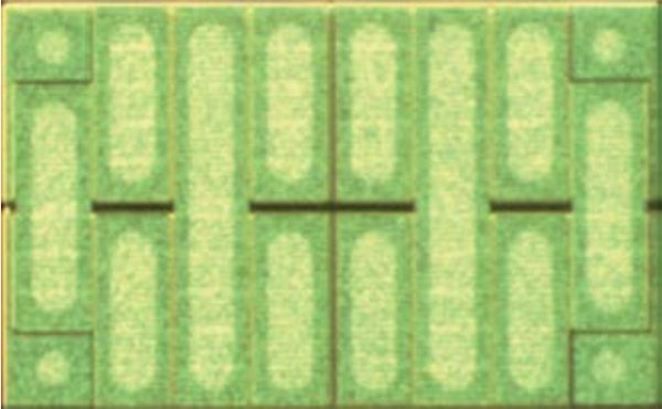
Figure 3: Four eGaN FETs integrated onto one chip.
In figure 3 is shown a product under development at EPC whereby four of those devices are integrated onto one chip. Not only does this integration save space on the PCB, but it also saves production costs and boosts the performance of the system (Look for these products in 2015). This type of innovation – the ability to integrate functions on a single chip – further increases the relative competitiveness of eGaN FETs compared with MOSFETs. Integration of discrete devices, however, does not necessarily increase the size of the market beyond the $12B occupied by discrete transistors, but allows eGaN FETS to attack that market in a more profitable fashion.

Figure 4: The evolution of eGaN technology from $12 B discrete transistors mounted on a printed circuit board, to integrated power devices, and finally to the 31.2B integrated power-plus-analog functionality Power Management Market.
To get at the larger, $31.2B, power management market, the next step to be taken is to integrate the analog IC functions that are the exclusive territory of silicon today. That step, illustrated in figure 4, is also under development and should be ready for customers in the 2017 time frame. The integration of power and analog functions yields additional cost and space savings and, even more significantly, it brings GaN’s superior performance to the analog circuitry driving the eGaN FETs. The replacement of the relatively slow silicon analog driver IC with an integrated GaN circuit enables a large boost in product performance – at a greatly reduced cost!
The $31.2B market for power management semiconductors is also just a stepping- off point on the way to addressing the entire $40B analog IC market and, potentially, the total $300B semiconductor market!
Has silicon reached the end of the road? Not yet, but a major challenge to silicon’s supremacy has finally surfaced after almost 60 years of silicon’s dominance.
About the Author
Alex Lidow is CEO and co-founder of Efficient Power Conversion (EPC), former CEO of International Rectifier and is the co-inventor of the HEXFET power MOSFET, a power transistor. He has authored numerous peer-reviewed publications on related subjects, and received the 2015 SEMI Award for North America for the commercialization of more efficient power devices. Lidow was one of the lead representatives of the Semiconductor Industry Association (SIA) for the trade negotiations that resulted in the U.S. – Japan Trade Accord of 1986 and testified to Congress on multiple occasions on behalf of the industry.