 Facebook
 Google
 GitHub
 Linkedin
Switched-Capacitor Converter Simplifies Migration from 1S to 2S Battery Architectures
This article discusses how switched-capacitor converter simplifies the migration of power-hungry devices from 1s to 2s battery architectures.
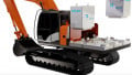
Power-hungry portable electronics are pushing battery capacities upward. As an example, mobile point-of-sale (POS) devices are built with integrated thermal printers that increase the power draw and may require a higher capacity battery.
A higher battery capacity is obtained by using more cells, in series or in parallel. For example, to double capacity, the easiest thing to do is to move from one cell (1S1P, i.e. 1S) to two cells in parallel (1S2P, i.e. 2P). This solution doubles the delivered power and preserves the voltage rating of the electronics downstream while increasing the current drawn from the battery. However, the problem comes when charging the battery since a standard USB-C cable is rated for 3A. Charging a 2P battery requires twice the current, which may exceed the 3A limit. Alternatively, the charging rate may be halved, leading to twice the charging time.

Figure 1: Mobile Point-of-Sale Terminal with a Thermal Printer
The USB Type-C standard supports 15W, 5V, 3A or 25W, 5V, 5A with a special electronically marked cable. But special cables and higher power adapters are both expensive and uncommon, so it is important for the application to support the standard 3A cable rating.
One way to meet this constraint and increase the power delivered is to use two Li+ batteries in series 2S1P, i.e. 2S rather than in parallel. Two series cells can be charged using the same current as a singlecell scenario and provide double the capacity. Now the problem is that your low-voltage charging and regulating electronics become incompatible and you must shop for higher voltage devices to connect the 2S battery to your system. This choice potentially creates problems in the availability of high-voltage devices and poses issues in inventory and the sourcing of charge and control devices of different voltage ratings. It also presents loss in purchase power due to volumes spread across different devices.
Alternatively, a 2:1 step-down converter (Figure 2) can be used to halve the 2S battery voltage and apply it to downstream low-voltage electronics. This way, the step-down converter can power the existing 1S circuits while enabling the use of 2S batteries.

Figure 2: 2S Low-Current Battery Management System with 2:1 StepDown Converter
In this design solution, we propose a 2:1 switched-capacitor converter (SCC) as the step-down converter of choice. The IC simplifies the migration to higher battery voltage by converting the 2S battery voltage to a 1S-equivalent output and allows designers to preserve the existing downstream 1S power architecture.
Why SCC?
The first thing that comes to mind for a step-down converter is the inductor-based buck converter. However, SCCs exhibit greater efficiency in a case like ours in which the ratio of the input voltage to the output voltage is an integer number (2). The SCC also has lower switching losses compared to an inductive buck converter. In the buck converter, each switch blocks the full input voltage and supports the full output current. In a 2:1 SCC, the switch only blocks half the input voltage resulting into lower switching losses. Finally, the SCC benefits from the significantly higher energy density of capacitors over inductors, resulting in a smaller PCB area. All the factors discussed above makes the SCC an ideal solution in this application.
SCC Operation
Figure 3 illustrates the two-phase SCC architecture. In the first cycle, FETs S1 and S2 are ON and CFLY1 is charged while supplying the load. Simultaneously, FETs S7 and S8 are ON, and CFLY2 is discharged to supply the load.

Figure 3: Operation of a 2-Phase SCC Architecture

Figure 4: SCC Waveforms of a 2-Phase SCC Architecture
Figure 4 shows the SCC waveforms corresponding to the first cycle illustrated above.
The next cycle is completely symmetric to the previous one: S1 and S2 are turned OFF while S3 and S4 are turned ON and CFLY1 supplies the load. At the same time, S7 and S8 are turned OFF while S5 and S6 are turned ON. CFLY2 is charged while also supplying the load. The two-phase operation reduces the ripple on the output capacitor.
The Switched Capacitor Converter
As an example, the MAX77932 is a two-phase switched-capacitor converter with integrated power switches that delivers 8A output current and divides the input voltage by two (see Figure 5). The IC is suitable for applications that utilize 2S Li+ batteries while powering circuitry that operates at a 1S-equivalent voltage. It is also suitable for applications migrating from 1S to 2S battery configurations and allows designers to preserve the existing downstream 1S power architecture.
High Efficiency
The SCC efficiency, shown in Figure 6, exceeds 98% at 0.5MHz switching frequency. Such high efficiency helps reduce heat losses and helps keep the application temperature below the ‘skin temperature’ level of discomfort.

Figure 5: SCC Block Diagram
With such a high efficiency, a two-stage solution made of one SCC and a low-voltage (LV) buck converter (LV DC-DC in Figure 2), will win against a single-stage high-voltage (HV) buck converter. In comparison to the HV buck converter, the LV buck operates with lower switching losses and a higher duty cycle. Table 1 represents the twostage solution advantage. To illustrate the effect of a 2% efficiency advantage, consider the case of a 12V, 3A, 36W charger, which is a common power level used in USB-C PD applications.

Figure 6: 2:1 SCC High Efficiency
The higher efficiency of the SCC solution results in approximately 0.7W lower heat dissipation. In this case, an IC with junction-to-ambient thermal resistance of 35°C/W will operate 25°C cooler without any thermal management material. This improved thermal performance makes it easier to keep the device ‘skin temperature’ within an acceptable range.

Figure 7: 2:1 SCC High Efficiency at Light Load
The IC has also an outstanding efficiency at low current. Figure 7 shows efficiency above 92% with currents in the 1mA to 10mA range. With portables spending extended amount of times in standby, this feature significantly enhances the battery life.
| TOPOLOGY | SCC EFFICIENCY |
BUCK EFFICIENCY |
OVERALL EFFICIENCY |
| SCC+LV BUCK | ~98% | ~94% | ~92% |
| HV BUCK | N/A | ~90% | ~90% |
Table 1: SCC Advantage
Small Footprint
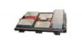
The IC is available in a tiny, lead-free 0.4mm pitch, 2.4mm x 2.8mm 42-pin wafer-level package (WLP). The combination of small chip and small passives yields a PCB footprint net area of only 14.6 mm². The comparison in Figure 8 shows a 27% footprint advantage compared to a competitor’s similar solution.

Figure 8: 27% Footprint Net Size Advantage
Frequency dithering
Switching noise from DC-DC converters can produce Electromagnetic interference (EMI) with a dominant frequency peak that disrupts radio signals or operation of other electronics nearby. The SCC offers a programmable frequency dithering mode to mitigate EMI. Dithering reduces the dominant peak and spreads the noise over a wide frequency band, making it easier for the device to comply with frequency emission standards.
Conclusion
The increasing power requirements of portable devices like mobile point-of-sale systems with thermal printers is pushing upward the capacity of their batteries. Although moving from a 1S configuration to a 2S configuration enables faster charging, it seemingly requires higher voltage downstream devices. The 1S downstream circuitry can be preserved by connecting the 2S battery to the system with a 2:1 step-down converter. We showed that for such a configuration, the switched-capacitor converter (SCC) yields the best overall system efficiency, reduces EMI with frequency dithering and is best suited for preserving the existing 1S downstream power architecture.
About the Authors
Bakul Damle is the Mobile Power business management director at Maxim Integrated. His current interests include battery and power management specifically in fuel gauges, energy harvesting, wireless charging, and battery authentication. He has several patents in test and measurement. Bakul holds a Master of Science degree in Electrical Engineering from the California Institute of Technology and a Bachelor of Technology in Engineering Physics from the Indian Institute of Technology.
Sagar Khare is the Mobile Power business manager at Maxim Integrated. He has wide-ranging experience in embedded power conversion, renewable energy, and battery management. Sagar holds a Master of Science degree in Electrical Engineering from Stony Brook University and a Master of Business Administration from Arizona State University.
Nazzareno (Reno) Rossetti is an analog and power management expert at Maxim Integrated. He is a published author and holds several patents in this field. Reno holds a doctorate in Electrical Engineering from Politecnico di Torino, Italy
This article originally appeared in the Bodo’s Power Systems magazine.


Made me a believer in the simplified SCC architecture in conjunction with a LV-bulk converter for 2S1P used for migration from 1S to 2S. In my simple mind and simply put, the higher the voltage for a given wattage = less amperage = lest amperage from the battery which in turn = longer run time. P =V/I