Facebook
 Google
 GitHub
 Linkedin
SEMIS An Interactive Tool for Selecting the Right Device for Your Application
This article introduces the benefits and features of ABB's Semiconductors Simulation (SEMIS, a web-based tool which is using PLECS software.
Semiconductors Simulation (SEMIS) is a web-based tool developed by ABB, which is using the PLECS software. It is intended to assist engineers at an early design phase in selecting the semiconductor device best fitting their application in respect to thermal losses. For a system designer it is important to choose the appropriate semiconductor according to the parameters of the application without having to spend too much time and effort.
SEMIS offers a user-friendly interface for parameter set up and provides a comprehensive steady-state analysis for the selected ABB semiconductors. Simulation results are obtained in both graphical and arithmetical form. Time-based graphs such as semiconductor current, output voltage, output current and temperatures are presented. The arithmetical results are listed in tables and among others indicate the estimated semiconductor switching and conduction losses as well as the junction temperatures. Input and output values for voltage and current are also available. Multiple device selection and simulation for the same conditions is possible for direct product comparison. Figure 1 provides an overview of SEMIS’ interface.
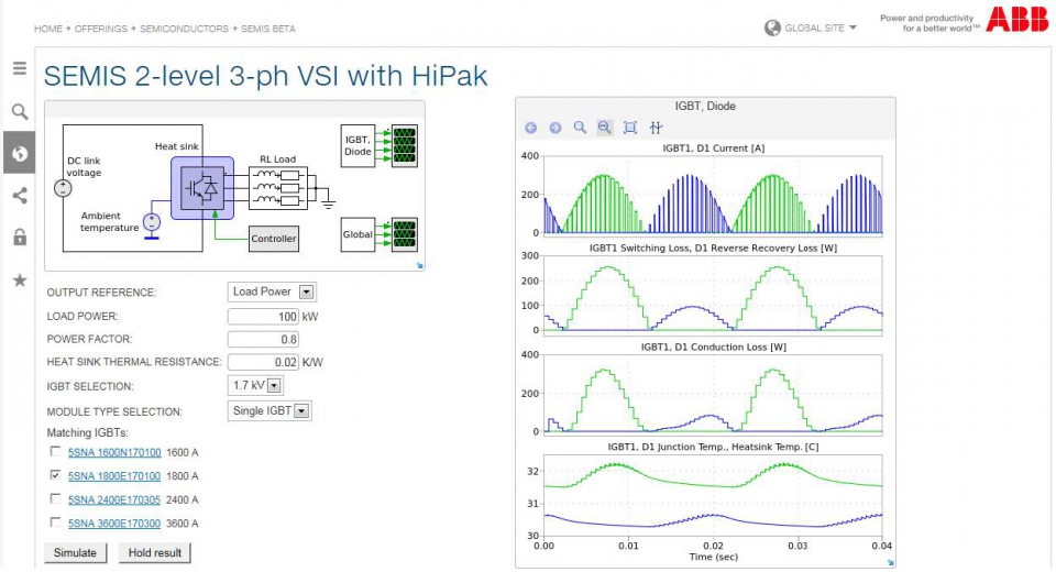
Figure 1: SEMIS interface overview
Features and functionality
Converter models
SEMIS aims to include the most common converter applications where the ABB semiconductor products are deployed. The first beta version is already available at the ABB Semiconductors website. It is a 2-level Voltage Source Inverter (VSI) feeding an RL-load. ABB HiPak IGBT modules can be selected for the simulation from a drop list. In the near future new circuits will be introduced for 3-level VSI with IGBT and IGCT based converters, which are currently under development (Figure 2).
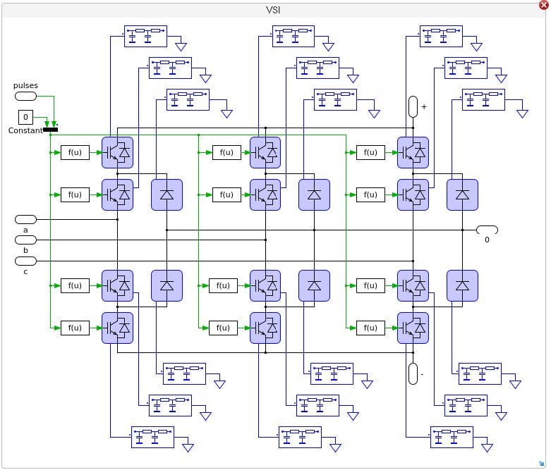
Figure 2: Upcoming 3-level inverter SEMIS thermal model
Thermal Model
In order to calculate the thermal behavior and junction temperatures, an accurate thermal description of the simulated semiconductor is needed. The thermal chain network considers the different packaging concepts (modules or press-pack products). Figure 3 shows the equivalent thermal model for IGBT modules available on the beta version. The values that are attributed for thermal resistance (Rth) correspond to the datasheet parameters of the selected product.
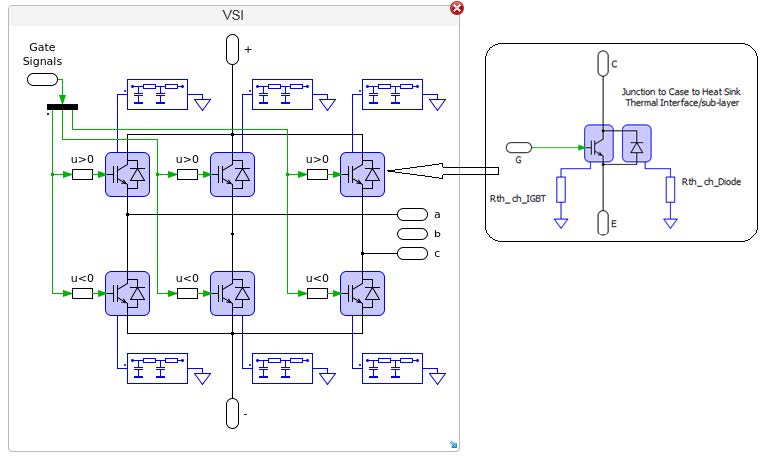
Figure 3: Converter and semiconductor thermal model
In SEMIS the thermal resistance between heat sink and ambient temperature RTH(h-a) is provided for a single switch per heat-sink
position, therefore the user needs to properly adjust the value of the thermal resistance of the selected heat sink to match the amount of
switches in the semiconductor package. For example, a heat sink with an Rth(h-a) of 10 K/kW is used with a HiPak1 IGBT module. This module consists of two switches as shown in Figure 4.
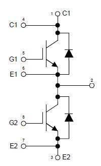
Figure 4: Dual switch IGBT module HiPak1
Each IGBT switch will get only half of the heat sink property and the effective Rth should be doubled, i.e. 20 K/kW. In other words, the user needs to multiply the heat sink value Rth(h-a) with a factor of 2 to account for each switch separately. For ABB’s HiPak IGBTs the possible electrical configurations are: single switch module, dual switch module, half-bridge and chopper module. The above consideration applies to the dual and half-bridge modules. Moreover, if multiple modules are put in parallel to the same heat sink then the same consideration needs to be accounted. Figure 5 shows how a dual IGBT switch in a half-bridge configuration is modelled in SEMIS.
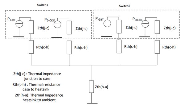
Figure 5: Dual switch IGBT thermal model
Working with SEMIS
SEMIS provides to the user a number of inputs for setting the conditions of the simulation similar to the actual application as shown in Figure 1. Electrical values for the load and control parameters for the switching of the semiconductor elements are such examples. The system designer can set optionally a desired Real Power or phase current rating as well as a Power Factor (PF) for the load on the AC side. For the control part, different Pulse Width Modulation (PWM) strategies are provided. The selection is done easily by clicking the various sections on the circuit and filling in the fields. The semiconductor selection is shortlisted depending on the selected blocking voltage rating and desired electrical configuration (e.g. single switch etc.). Figure 6 shows a functional flowchart of SEMIS.
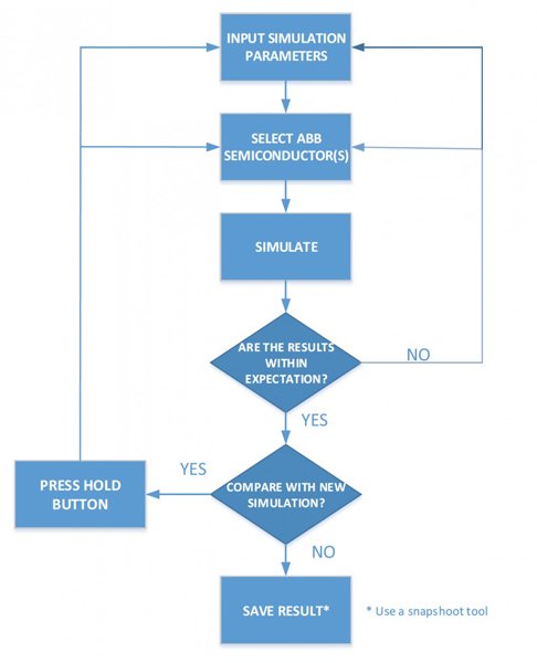
Figure 6: SEMIS functional flowchart
Output results
SEMIS simulation results are time-based graphs and tables with arithmetical values. The semiconductor losses are analytically calculated as switching and conduction losses. They are also presented on converter level, accounting for the total losses on all elements. Having the input power also available in the results, SEMIS calculates the total semiconductor losses as a percentage of the absorbed power from the converter. In this way, the user gets an indication of the impact of the semiconductor selection in the overall efficiency of the converter. The semiconductor junction temperature Tj is another parameter included in the results allowing for assessing the thermal limits of operation. If permissible limits are exceeded for the junction temperature Tj or if the applied voltage is out of the recommended limits of the product to be simulated, then alert messages are prompted. Figure 7 shows the different types of representations for the simulation results in the currently available beta version.
As mentioned, SEMIS is based on the PLECS software. Subsequently, it adopts the ideal switch model for the semiconductor behavior where the losses are calculated through a lookup table based on the ABB data sheet specifications for switching and conduction losses. Figure 8 shows this concept (courtesy of PLEXIM).
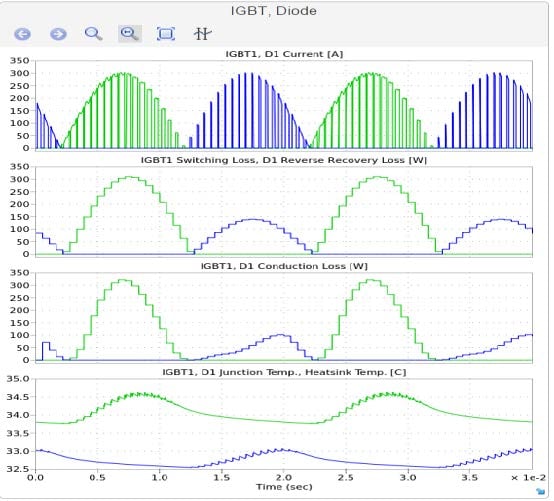
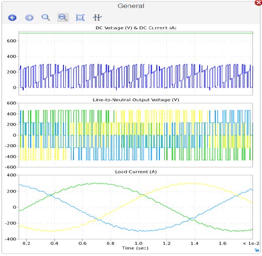
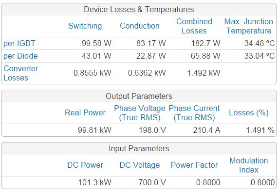
Figure 7: SEMIS simulation results
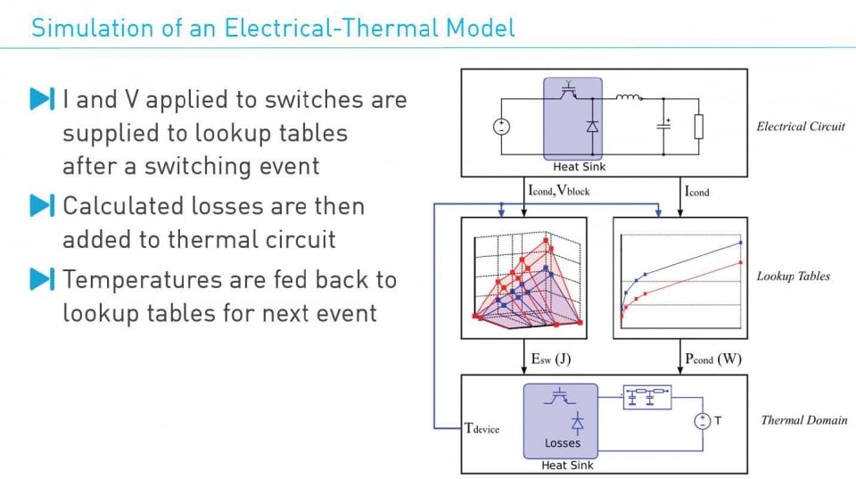
Figure 8: Lookup table method (courtesy of PLEXIM)
ABB Device Models
SEMIS uses the lookup tables, which have been created from the ABB Semiconductor’s datasheets. For each product available for simulation, a dedicated lookup table has been prepared for referencing the switching and conduction losses. These files are in the XML format and are available for downloading from the ABB Semiconductors website. An example of the content of such a lookup table is shown in Figure 9.
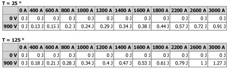
Figure 9: Indicative data in device lookup table
SEMIS next steps
The SEMIS simulation tool has been initially introduced through a beta version, which is to be updated to the final version soon. The basic platform will be the same and it will only differentiate in the sense that additional features will be included such as allowing for simulating an active load.
Upcoming converter models will include:
- Thermal simulation of a 3-level VSC with ABB HiPak IGBTs
- Thermal simulation of 3-level VSC with ABB asymmetric IGCTs
- More ABB semiconductor models will also become available in the XML format from the ABB website for PLECS users.
To start using SEMIS and downloading the available product models visit the ABB Semiconductors webpage.
About the Authors
Vasilis Kappatos worked as the Senior Application Engineer for Power Semiconductors at ABB Switzerland since April of 2014. Now, he works as the Bid and proposal engineer for MV drives since March 2018. He is highly skilled in the field of photovoltaics, solar energy, as well as electrical engineering field. He earned his Diploma as a Technologist Electrical Engineer at the Technological Education Institute of Piraeus where he was an apprentice at the industrial automation switchboards design and implementation department. He then earned his Diploma in Electrical and Computer Engineering, Power Systems, Power Electronics - Automation at the University of Patras.
Anup Kavimandan worked as an Associate Scientist at ABB where he was focused on power electronics, converter design, control and modulation, power semiconductor devices and development of innovative technologies in the areas of HVDC and FACTS solutions; working in close collaboration with R&D teams in Sweden, Switzerland and participate in Global R&D projects. he holds a Bachelor's Degree in Electrical Engineering earned at Indian Institute of Engineering Science and Technology. He also holds a Master's Degree in Electrical Engineering earned at the Indian Institute of Technology in Kanpur.
Evgeny Tsyplakov works as the Principal Application Engineer since April 2013 where he is skilled in the field of HVDC, Matlab and PCB design. He holds a Master's Degree in Electromechanics earned at MIIT at Moscow.
Madhan Mohan works as the Proposal Engineer at ABB since June 2015. He earned his Bachelor's Degree in Electrical and Electronics Engineering at the Thangavelu Engineering College located in Nadu, India.