Facebook
 Google
 GitHub
 Linkedin
Monolithic Current and Temperature Sensing in Automotive Qualified Bare Die IGBTs
This article describes the sensing circuitry and outlines the advantages for traction inverters in hybrid and electrical vehicles
650V automotive-qualified bare die IGBTs are aimed at power module manufacturers who are developing advanced solutions for automotive traction inverters.
The IGBT product family PCGAXX0T65DF8 includes versions for 160, 200 and 300A. Monolithic temperature and current sensing allows direct on-chip measurement of junction temperature and collector-to emitter current. The technique offers several advantages compared to off-chip temperature and current sensing. The article describes the sensing circuitry and outlines the advantages for traction inverters in hybrid/electrical vehicles (H/EV).
Traction inverters for H/EVs require power semiconductor devices with breakdown voltages in the range of 650V. Fairchild’s new product family of AEC-Q101 automotive-grade qualified bare die IGBTs is designed for applications in today’s and next-generation hybrid/plug-in hybrid, fuel-cell and battery-powered electric vehicles. We will refer to these vehicles simply as H/EV.
Fairchild’s bare die automotive-qualified IGBTs are based on the third generation of Field Stop Trench IGBT technology and are matched with a soft fast recovery diode qualified to automotive-grade standards with additional features and options, such as changing gate pad size and location to accommodate different diameters of aluminum wire, resizing the die and customizing the breakdown voltage.
The new bare die PCGA160T65NF8, PCGA200T65NF8, and PCGA300T65DF8 IGBTs can be available with or without integrated monolithic temperature and current sensing circuitry, in three current ratings of 160, 200 and 300A. Their breakdown voltage of 650V is guaranteed over a junction temperature range from -40 to +175 °C.
Bare die IGBTs are typically used by power module manufacturers who are designing their own solutions for H/EV traction inverters to achieve a high level of power integration and reliability, or special power interconnections. The overarching objective is to push the power limits beyond standard module products.
Power Device Challenges
When dealing with power semiconductors, designers are confronted with the following challenges:
- power loss
- thermal management
- short-circuit, overcurrent/overvoltage and overtemperature protection
- current measurement
Power losses are affected by the VCEon value of an IGBT, and by its switching behavior (turn-on and turn-off time) and switching frequency. These properties are impacted by the characteristics of the IGBT technology, the gate driving circuitry, the package stray inductance, and the thermal management system.
Since power losses can only be minimized but never fully eliminated, thermal management must aim to remove the heat created by the losses from the semiconductor. The best way to remove this heat is to improve the thermal conductivity between the silicon and the outside world. In recent, more advanced power modules the users are adopting sintering techniques for the top and bottom of the power device combined with double-sided cooling to improve thermal conductivity.
The next problem that designers are facing is protecting the IGBT against overtemperature, overvoltage and overcurrent. Overvoltage can be limited by controlling the amount of the stray inductance in the current path by the appropriate design and controlling the rate of change of the current.
Overcurrent and overtemperature are undesired occurrences that can happen in the life of the power semiconductor. Being able to detect and act upon them in time can extend the life of an inverter. Current measurement is required by the motor control system to control the amount of current and torque delivered by the motor.
Temperature Sensing
Monolithic integrated temperature sensing in bare die IGBTs is accomplished by measuring the forward voltage drop (VF) of a string of polysilicon diodes, which are fabricated monolithically on the same die as the IGBT. Because the VF value of a diode shows a well known and linear dependence on Tj (Equation 1 and Figure 1). The method of monolithic current sensing proves to be the best way to measure the IGBT’s junction temperature.
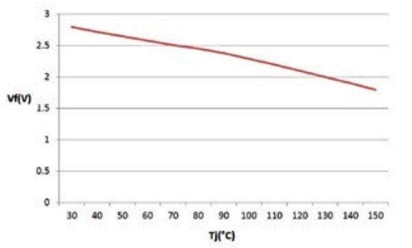
Figure 1: Dependency of voltage drop VF on the junction temperature Tj
The temperature sensor requires the diode to be forward-biased with precise constant current. The resulting voltage drop must be sensed and conditioned via an interface circuitry. Since the temperature diode is placed monolithically on silicon along with the power device, it is capacitive-coupled to the high voltage switching node of the IGBT.
The interface circuit must be designed to read the small temperature-dependent VF value, reject the switching voltages and pass the signal across an isolation barrier.
There are many ways of filtering the signal and passing it across the isolation barrier. An example is the use of an isolated amplifier and an analog-to-digital converter. This is combined with synchronous sampling to avoid the capturing of samples occurring with transient noise spikes. (Fairchild is preparing an Application Note dealing with the design of such an interface.)
Current Sensing
Monolithic integrated current sensing is accomplished by measuring the current of a small IGBT in parallel with the main IGBT and then multiplying it by a known scaling factor. IGBTs consist of thousands of cells in parallel via a metallization area on the top of the device. The small IGBT represents a portion of these cells that has been left disconnected from the rest of the cells and is made available as a current mirror.
The basic concept of the current sense function is shown in Figure 2. A separate emitter connection provides a fraction of the main collector current (IS), which is connected to an external resistor (RS). This connection generates a voltage drop, which is proportional to the sense current. The sense resistor voltage is used to determine the current, and by knowing the main collector current (IC), a “sense ratio” (Ratio) is computed, which is given by Equation 2.

Figure 2: The basic concept of the current sense function
The sense resistor (RS) can be replaced by an op-amp circuit that is designed to directly amplify the sense current in a current-follower configuration, thereby eliminating the sense emitter voltage bias.
The current sense ratio is temperature dependent, but, when combined with junction temperature sensing, it is expected that this interface will yield the necessary information to compensate for the junction temperature and produce a more accurate measure of the main collector current.
A bit more difficult is to correct the current dependency. This causes a limitation of the accuracy at low current, where low current are considered current levels below 10 percent of the full current range. The main limitation of monolithic current sensing is indeed the accuracy at a low current level. More details will be provided in the upcoming application note.
As mentioned above, monolithic current sensing can be put to various uses in an H/EV inverter. The most simple use is overcurrent protection, which may be accomplished easily with a comparator circuit. Such use can augment or replace the traditional desaturation protection.
A much more challenging and potentially valuable use is motor control, which is feasible with additional interface circuitry and intelligent processing in combination with on-die temperature sensing. This application of the monolithic current sense function is in active development at Fairchild. Figure 3 shows some initial results achieved with the on-die current sensing.
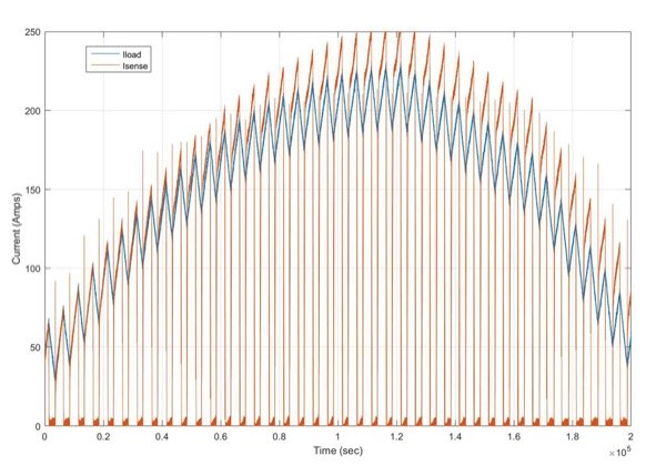
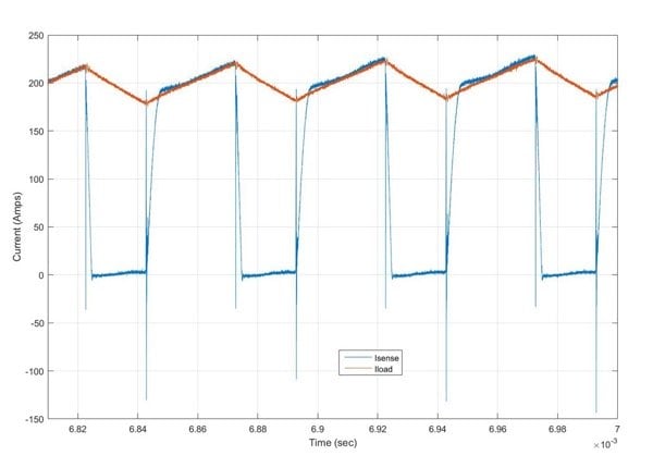
Figure 3: Some initial results achieved with on-die current sensing
Bare Die Layout for Sensing
An example of the bare die layout showing the temperature sense and current sense pads on the top side of the IGBT is given in Figure 4.

Figure 4: Layout of temperature and current sense pads on the top side of the IGBT
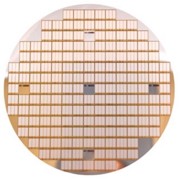
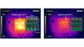
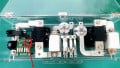
Figure 5: Wafer with bare-Die IGBTs as presented at PCIM Europe, 2016
In conclusion, monolithic integrated current sense and temperature sense circuitry provides a reliable way of measuring the junction temperature of an IGBT in power module applications, and of the collector current - without additional sensors. These techniques can provide substantial advantages for module manufacturers. It simplifies the sensing of key parameters, reduces component count, achieves a faster response to hazardous operating conditions, allows a more precise determination of junction temperature, leads to better utilization of the power silicon, and increases reliability. All of these characteristics will help inverter manufacturers or vehicle OEMs to achieve a more competitive position in the marketplace.
This article originally appeared in the Bodo’s Power Systems magazine.
About the Authors
Fabio Necco is Director of Product Line Management, Hybrid & Electric Vehicle segment at Fairchild Semiconductor. He is responsible for Fairchild’s worldwide strategy for the Automotive HEV/EV segment. Lead activities from product definition to product development for high voltage and high current power train/drive train automotive solutions. He is particularly skilled in the field of integrated circuits and semiconductors. He earned his Master's Degree in Microwaves Electronics and Measurement Systems at the Polytechnic University of Turin located in Italy. He also earned a Sequential Certificate in Project Management at the University of California.
Roy Davis is Manager of Advanced Systems Design and Development at Fairchild Semiconductor. He is responsible for managing and operating the automotive power electronics laboratory in Ann Arbor, supervising a small staff in support of Fairchild's automotive power module business. He is skilled in the field of simulations, power electronics and electrical engineering. He earned his Bachelor's Degree in Electrical Engineering at Michigan Technological University. He then earned his Master's Degree in Electrical and Computer Engineering at the University of Michigan. He then finally acquired his PhD in Mechanical Engineering at the University of Wisconsin-Madison.