Facebook
 Google
 GitHub
 Linkedin
Modern Clamping Systems for Testing Power Semiconductor Devices
This article describes the steps of development and research carried out to design a clamping system for disc semiconductors and analyzes the encountered issues
Power semiconductor devices have many parameters and characteristics that must be measured using specialized equipment. The design of such equipment must account for many factors such as reliability, flexibility, ergonomics, and attention to overall aesthetics. This article describes the steps of development and research carried out to design a clamping system for disc semiconductors and analyzes the encountered issues. A number of technical solutions were used to improve ergonomics, later proving their efficiency in real operation.
Today power semiconductor devices are the fundamental design elements of various equipment in many industries. Power electronics is constantly evolving and improving, therefore, requirements to the accuracy of measuring their main parameters are also increasing. The Automation Laboratory at the R&D Center of Proton-Electrotex JSC has developed a lineup of test equipment designed to measure parameters of power semiconductors meeting all requirements to accuracy, reliability, and ergonomics. It is capable of measuring the following parameters for bipolar semiconductors:
- Parameters in open state: VTM, VFM, ITSM, I FSM, IL;
- Blocking parameters: VRRM, VDRM, VDSM, VRSM, IDRM, IRRM, (dVD/dt)crit;
- Gate parameters: VGT, IGT;
- Thermal parameters: Rth, Zth;
- Dynamic parameters: QRR, tq,tgd.
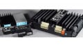
The test equipment (Fig. 1) is a complex including a clamping system and individual measuring units installed in a 19” rack. Each block performs a specific function. Control is carried out using a HMI unit with a 17” capacitive touch screen. The software allows to make several successive measurements in automatic mode. The complex is serviced by one operator. The operator’s responsibilities include selection of the measurement profile, installing the device under test in the clamping system and launching the tests with the "Start" button.

Figure 1: The tester with the clamping system
Previously the company used test equipment with a number of drawbacks. To make a series of measurements it was required to switch from one test station to another resulting in much lower productivity. Each station occupied production area and required more operators. The operator had to manually adjust the equipment to the required test conditions before each measurement. The clamping systems were based on a pneumatic actuator with several disadvantages: insufficient force to clamp large diameter devices, the inability to dynamically change the speed and force of clamping.
To eliminate these main disadvantages, the Automation Laboratory has developed a state-of-the-art clamping system. The tester consists of two standard 19” racks with measuring units and a clamping system inside. This modular design made it possible to customize the equipment for a specific task by selecting the units needed in the tester. Besides, it made maintenance and repair of the equipment much more convenient significantly reducing the downtime. It is only needed to disconnect the failed unit and replace it with a backup, then the complex is ready for continued operation. Automation of the measurement process minimized the influence of the human factor on the quality and reliability of measurements, while the work of the operator became less critical.
Ergonomics and aesthetics were also considered. Initially, the clamping system was designed as a separate mechanism connected to the tester, but this configuration resulted in unused space in the rack above the clamping system. Some units need to be connected with the shortest possible conductors (cables and buses) to ensure precise measurements, so it was decided to include the clamping system in the tester and place the measuring units in the free space above it.
The operator’s workplace includes a touch screen, clamping system and a table to put the devices. For convenience, the touch display is detached from the tester on a bracket, allowing the operator to adjust its position as needed. Several ergonomic improvements were made after a survey of operators from the manufacturing. A recess for leg space was made in the housing at the operator’s workplace. It was also revealed that the clamping system provides insufficient lighting for the operator to control the process of clamping the system and to track wear of the contact surface. The clamping system was analyzed for the required lighting conditions and light sources were selected and installed both inside and outside the tester.
The measuring and auxiliary units (Figure 2) are placed in housings of various heights designed for a standard 19” rack. Light indicators on the frontal panel inform about the correct operation, while connectors and output buses are located on the rear. To increase the accuracy of measurements a bifilar arrangement of buses is used, both inside and outside the unit.

Figure 2: Measuring and auxiliary units
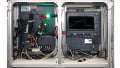
The clamping system included in the tester (Fig. 1) is designed to clamp disc diodes, thyristors and separate basic units. The device provides an even distribution of pressure across the entire area of the semiconductor’s contact surfaces. It is a separate mechanism consisting of a frame, a drive, a misalignment compensation system and a control unit. The maximum force of 150 kN is enough to clamp large-diameter devices up to 150 mm.
Large-diameter devices have a weight of almost 3 kg. It is physically difficult for the operator to manipulate such a device, and having to use both hands increases the chance of damaging the surface of the device during installation and positioning. To measure the device in the hot state, the preheated device is installed in the clamp between two contact surfaces heated to 190 °C. In case of large-diameter devices this task becomes extremely difficult and dangerous. To resolve this issue, it was decided to equip the clamping system with a draw-out loading system. The lower contact surface automatically extends after the measurements are complete (Figure 3) allowing to easily install a large-diameter device or a device in hot state. The system is equipped with a sensor monitoring the position of the contact surface. If the surface is not properly retracted, the safety system will engage and an error will be shown on the display. For structures and semiconductors of small diameter with weight from 70 to 1000 g, it is much simpler and faster for the operator to install them in the clamp with one hand or tweezers, while the draw-out system will be unnecessary and take extra time. When needed, the draw-out system can be turned off using the touch screen.
To draw out the lower stand and to move the middle plate of the clamp it is necessary to disconnect the bifilar power line. A pneumatic contactor was developed and tested for this purpose. It provides reliable current flow without burning and sticking its contact surfaces.

Figure 3: The clamping system with extended draw-out system
Poor contact surface of the clamping system (Figure 4) can damage the exterior of a semiconductor device and it would need to get scrapped. Therefore, the replaceable upper and lower contact surfaces have a high tolerance for flatness and a roughness of Ra 0.8. For convenience, the surface is quickly detachable, so that replacement of damaged or worn replaceable plates requires short downtime of the equipment. A worn replacement plate can pass grinding and then it can be used again in the clamping system.

Figure 4: Contact surfaces of the clamping system
For high-amplitude current pulses it is critically important to ensure even distribution of force throughout the contact surface of the semiconductor. Since the areas with concentrated force have minimal resistance and the current flows along the path of the least resistance, high current pulses can cause local overheating and failure of the device. To solve this problem, a system was created to compensate the misalignment of the contact surfaces, thereby increasing the uniformity of the force distribution and, thereby, the current flow through the contact surface of the device. The upper and lower contact surfaces are mounted on spring-loaded hinges. If the surfaces were not parallel before clamping, they get aligned due to spring-loaded hinges. To compensate for the plane-parallel movement that occurs during this alignment, the lower contact surface is mounted on a thrust bearing. This solution improves the distribution of force and reduces the likelihood of damage to the device. The contacts are connected to the power bus with highly flexible braided wire (6th class of flexibility). Using such a flexible connection provides free movement of the compensation system.
The initial design had a single hinge on the lower contact surface, but a large number of tests and trial operation demonstrated inadequate force distribution and a high chance of damage to small-diameter devices, so it was decided to add it to the upper contact surface too. Figure 5.1 shows the force distribution between the device and the contact surface of the clamping unit with one hinge, and Figure 5.2 with two hinges.

Figure 5.1: а – upper contact surface; b – lower contact surface.

Figure 5.2: а – upper contact surface; b – lower contact surface.
Figure 5: Force distribution between the contact surface and the semiconductor
The clamping system is equipped with a servodrive allowing to control the clamping speed and position of the lower contact surface. For higher productivity, the clamping is divided into stages. Initially the drive develops maximum speed, but then the speed is reduced before the moment of clamping to prevent impact and damage to the device under test. The clamping system has an electromagnetic brake that can maintain maximal force for a long period with high accuracy without putting the load on the drive, making it possible to carry out longterm measurements and significantly increase the drive's service life. The drive mechanism is based on a ball screw capable of developing high force and high accuracy of vertical positioning of the device.
The device is also equipped with a heating system to take measurements in the hot state. A ring heater around the contact surface was selected for this purpose since such arrangement does not affect the force distribution. Cartridge or spiral heaters require to make mounting holes in the base of the contact surface resulting in distorted force distribution. Flat heaters were excluded as they are not designed for heavy loads. The heating system is capable of reaching and maintaining a given contact surface temperature of up to +200°C. A temperature regulator and thermal resistance sensors are installed in the measurement zone to maintain and control the temperature.
The clamping system is equipped with potential contacts to measure static losses. They are located in the center of the contact surfaces. The first version had spring-loaded contacts that did not produce expected results. The contact operates at high temperature and experiences mechanical stress during installation. The self-made contact often failed due to sticking, burning and damage, so it was decided to increase reliability by using ready-made spring contacts. Several alternatives were reviewed for this purpose and a series of tests was carried out. The contacts were selected based on dimensions, thermal parameters and spring elasticity. The upper threshold of the operating temperature was at least +200°C. The spring elasticity was chosen based on the weight of the smallest device so that the spring elasticity did not exceed its weight, so a contact was chosen with spring force of not more than 0.8 N. After long-term operation of the selected contacts from several manufacturers to compare their reliability it was decided to use spring contacts made by INGUN.
For operator’s safety, an optical safety shutter is installed to prevent access to the working area of the clamping system during testing. Its operation is based on a light curtain of infrared rays formed between the emitter and the receiver located on the same axis. If the beam gets blocked during the device clamping and measuring procedure, it sends a signal to the commutation unit which disconnects the measuring units by hardware and connects the tested device to protective ground, so that the accumulated charge cannot harm the operator. Then the signal is sent to the control unit of the clamping system and the clamping process is suspended. The whole process of stopping measurements and turning off the clamping system takes place in a split second. The emergency stop button located in front of the operator’s workplace in easily accessible place works in the same way.
Design of the tester also accounts for the influence of the electromagnetic field loop that is formed when the current flows through the power buses and contacts of the clamping system. A bifilar arrangement of power buses and a material with a low magnetic permeability index were chosen to minimize its effect on measurements. Initially, steel 40X13 was used as the material of the contact surface resulting in transformation effect or the effect of electromotive force induced to the potential removal line. To understand how this effect occurs, consider the system and the principles of the transformer operation. It is based on the phenomenon of electromagnetic induction. This phenomenon arises from the presence of an alternating magnetic field; it is created in a magnetic circuit consisting of a flux guide with electric windings. One winding is connected to an AC source and is called primary, the other winding is used to remove voltage to power the load, this winding is called secondary. If an alternating voltage is applied to the primary winding, alternating current will flow through it, creating an alternating magnetic field around the winding and in the flux guide. It forms a magnetic flux, which passes through the flux guide and crosses the primary and secondary windings and inducing alternating electromotive forces in them.

Figure 6: Diagram of creating a parasite transformer in the clamping system
The clamping system has a power current circuit that passes through the device under test and forms the primary winding of the parasite transformer (Fig. 6). It is necessary to measure the voltage drop that occurs on the power semiconductor device when the power current flows. It is achieved using potential spring contacts located in the center of the upper and lower contact surfaces, which form the secondary winding of the parasite transformer together with the wires. The core of the parasitic transformer is formed by contact surfaces. The additional electromotive force occurs on potential lines as follows. The power current flows through the device along the power circuit and an alternating magnetic field arises, the lines of which are directed according to the screwdriver rule. Accordingly, concentration of the magnetic field in the space between the buses is higher since the magnetic field created by the power conductors is added up. The magnetic field is much weaker at the point where the potential wires are located because it is farther from power buses. Using martensitic steel 40X13 with high magnetic permeability index as the contact node material enhanced the transformation effect. Therefore, it was decided to use D16T aluminum alloy as the main material of the contact unit, and to make the replaceable plate from austenitic 12H18N10T stainless steel. These materials have a low magnetic permeability index. Steel 12X18H10T is hard enough to use as a contact surface. The aluminum alloy D16T is not suitable for the contact surface, as it is a soft material. Using it results in traces remain on the contact surface in after several clamping operations, causing damage to the surface of the device.
To summarize, the test equipment developed and manufactured by the Automation Laboratory of Proton-Electrotex JSC meets the requirements of a wide range of consumers. Modular design of the testers allows the customer to select all the necessary parameters. Using components of well-known leading manufacturers ensure reliability of the equipment. Each case of negative feedback acquired during operation was followed by an in-depth analysis (FMEA – failure mode and effects analysis). This approach allowed to offer high-quality ergonomic equipment.
About Proton-Electrotex
Proton-Electrotex is one of the Russian leaders in the design and manufacture of power semiconductor diodes, thyristors, modules, coolers, IGBTs (IGBTs), as well as power units for use in various electric energy converters. The company was founded and began production in 1996 on the leased premises of the Proton plant. Since then, Proton-Electrotex has developed its own infrastructure for the entire production cycle. Production is equipped with modern production lines, measuring equipment of our own production and areas for “clean technologies” with full compliance with the requirements for electronic products and microelectronics.
Sources
- Yablonskiy A. A., Nikiforova V. M. Kurs teoreticheskoy mehaniki. 16th edition — M.: KnoRus, 2011. — p. 608.
- Gulia N. V., Klokov V. G., Yurkov S. A. Detali mashin. — M.: Publishing center "Akademiya", 2004. — p. 416.
- Apollonskiy, S. M. Teoreticheskie osnovy elektrotehniki. Elektromagnitnoe pole / S.M. Apollonskiy. - M.: Lan, 2012. – p. 592.
This article originally appeared in the Bodo’s Power Systems magazine.