Facebook
 Google
 GitHub
 Linkedin
App Advantages of Intelligent IGBT Gate Drivers in 3300Vac Mine Inverters
In recent years, the coal mining industry has re-entered a period of rapid development, and the demand for the core equipment for coal mining, 3300 Vac high power inverters, is growing.
This article is published by EEPower as part of an exclusive digital content partnership with Bodo’s Power Systems.
IGBT and gate driver play a crucial role as the core components of the inverters. At the early stage, IGBT gate drivers in the industry were dominated by imported analog gate drivers. As the development of digital gate driver technology is mature, the demands of high reliability, miniaturization and intelligence can be better satisfied, the application is more and more widespread. According to the NPC I-type 3-level topology characteristics and application challenges of 3300 Vac inverters, Firstack targeted developed a new generation of intelligent IGBT gate drivers, which can effectively solve the problems of the incorrect turn-off timing of the inner and outer IGBTs, too high turn-off overvoltage of inner IGBT, and the large turn-off delay time of high-voltage IGBT module, etc. Additionally, the IGBT gate drivers can satisfy the intelligent maintenance needs by intelligent fault communication technology.
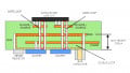
The 3300 Vac coal mine inverters, shown in Figure 1, are mainly used for heavy-duty soft starting and intelligent speed regulation in coal mine scraper conveyors, belt conveyors, and transfer machines. Its power ranges from 500 kW to 2600 kW, which belongs to high-voltage, high-power electronics equipment. The main topology scheme is the NPC I-type 3-level with the 4500 V IHV IGBT package module, as shown in Figure 2.

Figure 1. (a) 3300 V coal mine inverter. Image used courtesy of Bodo’s Power Systems [PDF]

(b) 3300 V coal mine inverter with motor together. Image used courtesy of Bodo’s Power Systems [PDF]

Figure 2. (a) One phase topology of the 3300 Vac inverter. Image used courtesy of Bodo’s Power Systems [PDF]

(b) 4500V IHV IGBT module and gate driver. Image used courtesy of Bodo’s Power Systems [PDF]
For NPC I-type 3-level applications with high-power IGBT, challenges follow at the IGBT module and gate driver technology levels.
The problem of turn-off timing of the inner and outer IGBTs is that the outer IGBT has priority over the inner IGBT to turn off, especially in the case of a short-circuit fault or undervoltage fault. The Vce short-circuit protection time of the traditional analog gate driver is too long, which leads to the inner IGBT under short-circuit condition withstanding a long short-circuit time that exceeds the safety range. In other words, there is a great risk.
Too high turn-off overvoltage of inner IGBT: Since the topology is more complex than the traditional 2-level topology, there is a large commutation loop in the inner IGBT, and the actual high-power module design has a large stray inductance in the busbar, which can easily lead to the module damage due to the high turn-off overvoltage. At the same time, in some applications, the space is very compact, and part of the design can not add absorption capacitors, resulting in the turn-off overvoltage being more of a problem.
Large switching delay for high-voltage IGBT modules: some high-voltage IGBT modules have excessive switching delays, leading to great challenges in dead time setting and waveform quality control.
Demand for IGBT intelligence maintenance: 3300 V coal mine inverters are generally installed in the mine shaft. When an IGBT module fails, whether it can quickly locate the cause of the failure is critical for reducing maintenance costs. At the same time, it is an important way to improve the benefits for equipment manufacturers to dominate the maintenance market in the increasingly fierce business competition environment.
IGBT Gate Driver Application Challenge
Turn-Off Timing of the Inner and Outer IGBTs
As shown in Figure 3, in the NPC I-type 3-level topology, there are six power devices in each phase: 4 IGBTs (S1, S2, S3, S4) and two diodes (D5, D6). Different switching combinations of the 4 IGBTs can be composed of different commutation modes, and the states of S1~S4 are represented by 0 and 1, respectively; 0 represents turn off, and 1 represents turn on. At the same time, the positive potential of the bus is “+1”, the negative potential of the bus is “-1”, and there are several combinations of modes (assuming the current flows inward), as shown in Table 1.
Table 1. Mode combinations
|
S1 |
S2 |
S3 |
S4 |
Hexadecimal |
Output |
|
1 |
1 |
0 |
0 |
C |
+1 |
|
0 |
1 |
0 |
0 |
4 |
+1 |
|
0 |
1 |
1 |
0 |
6 |
0 |
|
0 |
0 |
1 |
0 |
2 |
0 |
|
0 |
0 |
1 |
1 |
3 |
-1 |
|
0 |
0 |
1 |
0 |
2 |
0 |
|
0 |
1 |
1 |
0 |
6 |
0 |
|
0 |
1 |
0 |
0 |
4 |
+1 |
|
1 |
1 |
0 |
0 |
C |
+1 |

Figure 3. NPC I-type 3-level topology. Image used courtesy of Bodo’s Power Systems [PDF]
As can be seen in Table 1, there are five modes in the NPC I-type 3-level, including steady-state C, 6, 3 and transition state 4, 2, where the steady-state C, 6, 3 follows the principle of complementarity of S1 and S3 and complementarity of S2 and S4. To analyze the timing problem, mode three is taken, at this time the state of S1~S4 is: 0011, as shown in Figure 4a, S3 and S4 are open, and the current flows from AC to the bus negative, at this time the AC point potential is “-1”. If there is a normal shutdown or abnormal overcurrent, which of the inner IGBT S3 or the outer IGBT S4 should be turned off first?

Image used courtesy of Bodo’s Power Systems [PDF]

Image used courtesy of Bodo’s Power Systems [PDF]

Figure 4. Image used courtesy of Bodo’s Power Systems [PDF]
Figure 4(b) shows that the outer IGBT is turned off first (S4=0), after which the current flows back to point O through D6 and the AC potential is “0”, and then the inner IGBT is turned off (S3=0), and the inner IGBT S3 is subjected to 1/2VDC at both terminals. Figure 4(c) shows that the inner IGBT is turned off first (S3 = 0), after which the current flows through D1 and D2 back to the bus positive, AC potential is “+1”, and then turn off the outer IGBT (S4 = 0), the voltage across the inner IGBT S3 is VDC, the module will damage due to overvoltage.
Based on the above analysis, the NPC I type 3-level must turn off the outer IGBT before turn-off the inner IGBT, either under normal shutdown conditions or under abnormal conditions. Under normal operating conditions, it is relatively easy to achieve timing turn-off through the control board. However, under short-circuit fault conditions, there are great challenges in the timing; the traditional analog gate driver scheme (e.g., PI) is based on Vce short circuit protection and active clamping function while assisting the master computer to coordinate the turn-off timing to complete. In this protection scheme, when there is a short-circuit fault in the inner IGBT, it will turn off first by itself, which results in overvoltage of the inner IGBT due to the turn-off timing error. However, the inner IGBT active clamping function will clamp the voltage at both terminals of the IGBT, and at the same time, the master computer will be informed of the inner IGBT short-circuit fault. After learning of the fault information, the master computer immediately turns off the outer IGBT first and then the inner to ensure the corresponding turn-off timing under the condition of the inner IGBT, not overvoltage. In the above protection scheme, the traditional driver will have the following problems.

Figure 5. Short-circuit test of high voltage module with 3-level topology. Image used courtesy of Bodo’s Power Systems [PDF]
First, due to the Vce short-circuit protection response time of the traditional gate driver is generally about 8 μs; in extreme cases, it will lead to the inner IGBT withstanding a long short-circuit time that exceeds the safe range under short-circuit conditions. Figure 5 shows the short-circuit condition test of the PI analog gate driver product based on a 4500 V/1200 A IHV module in NPC I-type 3-level topology. S3 is the inner IGBT, and S4 is the outer IGBT. As is the test waveform, the outer IGBT is turned off first, and then the inner IGBT, but the outer IGBT withstands the whole short-circuit time of 14 μs, more than the module safety limit of 10us, which means there is a great risk.
Second, the traditional gate driver generally uses the basic active clamping technology, and the clamping circuit has the problem of inaccurate clamping voltage, specifically shown in Figure 6(a). The basic active clamping circuit, which is directly connected to the IGBT C and the gate G through a certain number of TVS, when the IGBT is turned off, once the turn-off overvoltage exceeds the clamping threshold of the TVS, the TVS breaks down. The breakdown current will be injected into the gate, leading to the gate Vge voltage rising and delaying the IGBT turn-off so the turn-off overvoltage energy will be consumed through the IGBT loss, and the TVS clamps the turn-off voltage. However, in the actual turn-off process, the last level of the push-pull circuit of the gate driver is connected to the -15 V power supply. There is a low-resistance path for the TVS breakdown current, which will lead to a large fluctuation in the current flowing through the TVS. According to the TVS V-I characteristic curve, as shown in Figure 6(b), when the current flowing through the TVS fluctuates drastically, the clamping voltage of the TVS also fluctuates drastically, resulting in inaccurate clamp voltage.

Figure 6. Basic active clamping circuit. Image used courtesy of Bodo’s Power Systems [PDF]

V-A characteristic curve of the TVS. Image used courtesy of Bodo’s Power Systems [PDF]
To solve the problems inherent in the basic active clamping technique, PI introduced the dynamic, advanced active clamping DA2C technique, as shown in Figure 7(a). Compared with the traditional basic active clamping technique, the current at the time of TVS breakdown is sampled via the CS circuit, and according to the current, the gate push-pull circuit is adjusted to the switching state of the -15 V power supply, and when the current at the time of TVS breakdown is smaller than the set threshold, the push-pull circuit is connected to the -15 V power supply. When the TVS breakdown current is larger than the set threshold, the push-pull circuit is cut off from the -15 V power supply, which removes the low-resistance path. This can effectively control the TVS current, thus effectively controlling the clamping threshold of TVS, which makes the clamping voltage more accurate. Figure 7(b) is the test waveform under short-circuit conditions for the PI analog driver products based on the Infineon FF1400R12IP4 module, and the Vce voltage is clamped at about 750 V at the turn-off moment.

Image used courtesy of Bodo’s Power Systems [PDF]

Figure 7. Advanced active clamping circuit Test waveform under short-circuit conditions. Image used courtesy of Bodo’s Power Systems [PDF]
Compared to the basic active clamping, dynamic, advanced active clamping DA2C can effectively suppress turn-off overvoltage. The clamping effect is great, but the voltage clamping process will be accompanied by a gate repeatedly turned on and off during a very short period, generating a certain amount of electromagnetic oscillation inside the module, which is a hazard for the safe operation of the module. During the actual action, the TVS current and power consumption are still large, if the active clamping circuit operates for a long period, the life and reliability remain a big challenge.
Too High Turn-Off Overvoltage of Inner IGBT
As shown in Figure. 8(a), the NPC I-type half-bridge operates in mode 6, the switching state of S1~S4: 0110, and the current will flow from the AC point to the “O” point through S3, D6. At this time, switch to mode 4, that is, S1 ~ S4 switching state: 0100, the current will flow from the AC point through the S2, D1 to the bus positive, in the turn-off process of S3, as shown in Figure 8(b), the entire commutation circuit passes through the C1, D1, S2, S3, D6 devices, which forms a large commutation loop with a large stray inductance. The NPC I-type 3-level scheme based on the IHV package uses six modules to form a phase of the bridge arm; the modules are connected by laminated busbars, as shown in Figure 8(c); the actual large commutation circuit needs to pass through the module and the corresponding laminated busbar, further increasing the stray inductance. According to the system measurement, it is generally up to 200 nH, much larger than the module recommended 30 nH, making the turn-off overvoltage abnormally high, and the module will fail easily due to overvoltage.

Image used courtesy of Bodo’s Power Systems [PDF]

Image used courtesy of Bodo’s Power Systems [PDF]

Figure 8. Image used courtesy of Bodo’s Power Systems [PDF]
In some applications, the volume requirement is higher, and an absorption capacitor cannot be added, so the traditional analog drivers can only rely on the active clamping function. Based on the active clamping technology, the actual application of the clamping effect is affected by bus fluctuation, temperature, and other factors, and due to the large stray, the active clamping often acts under some of the normal operating conditions, resulting in the clamp diode a risk of failure, which brings hidden dangers to the reliable operation of the IGBT.
Large Switching Delay for High-Voltage IGBT Modules
The IHV package IGBT used in 3300 V inverters belongs to the high-end module in the industrial field of semiconductor modules, and the market can supply relatively few products. In the face of growing demand for equipment, the supply will fall short of demand. Due to the different technical routes of various module manufacturers, some manufacturers of IGBT have switching delay problems, such as the turn-off delay of the 4500 V/1200 A module of A manufacturer is about 7 μs, as shown in Figure 9, while some of the controller’s dead time setting requirements are <4 μs, which brings a great challenge to the controller’s dead time setting.

Figure 9. Tdoff time of the module of A manufacturer tested at VDC=2000 V, IC=1500 A. Image used courtesy of Bodo’s Power Systems [PDF]
Demand for IGBT Intelligence Maintenance
Compared with the traditional 2-level, there are 12 IGBTs in the 3-level inverter, which is twice as the 2-level, and each IGBT has at least two types of faults: Undervoltage and short-circuit, which makes a total of 24 types of faults. The traditional analog gate driver can’t distinguish between Undervoltage or short-circuit faults, which leads to a big challenge in analyzing the whole machine when problems occur in the actual R&D and debugging or the field, because only the IGBT faults are reported, not including the type of faults. At present, the IGBT gate drivers of 3300 V inverters of most manufacturers are standard analog gate drivers of PI; there are no protection measures for IGBT failure after-sales maintenance of inverters, which can not meet the equipment manufacturers’ demand of targeting the maintenance market through intelligent technical means.

Image used courtesy of Bodo’s Power Systems [PDF]

Figure 10. di/dt detection principle diagram Intelligent gate driver with di/dt detection. Image used courtesy of Bodo’s Power Systems [PDF]
Key Technologies of Intelligent IGBT Gate Driver
In response to the problems above in applying high-voltage IGBT in 3300 V coal mine inverters, Firstack has developed a new generation of plug-and-play intelligent IGBT gate drivers: the HV1027P. Compared with traditional analog gate drivers, there are the following features brought about by digital innovation.
Fast Short-Circuit Detection Based on di/dt
As is the timing control of the inner and outer IGBT shown earlier, especially in the short-circuit state, the earlier the short-circuit protection is performed, the safer the inner and outer IGBT of the NPC I-type 3-level are. The intelligent gate driver uses a fast short-circuit detection technology based on di/dt, the basic principle shown in Figure 10 (a). Inside the module package, there is an equivalent stray inductance LPE in the power E terminal and auxiliary E terminal, which is generally around 5-10nH, and the change di/dt of the current flowing through the IGBT will produce a voltage drop V on the LPE, which is calculated by:
\[V=L_{PE}\times di/dt\]
Since the di/dt of the current under normal conditions is generally at 10A/μs, while the di/dt under short-circuit conditions is at 1000 kA/μs, the voltage drop difference produced is very large. The gate driver will be able to quickly determine whether short-circuit protection occurs and provide effective protection by detecting the voltage drop V. As shown in Figure 10(b), the gate driver has added a reed mounted on the power E terminal of the module for the di/dt protection detection function.

Image used courtesy of Bodo’s Power Systems [PDF]

Figure 11. Top: Based on Vce short-circuit detection. Bottom: Based on di/dt short-circuit detection. Image used courtesy of Bodo’s Power Systems [PDF]
As shown in Figure 11, the short-circuit protection process based on Vce detection and di/dt detection are given, respectively. From the test waveform, the protection time based on Vce short-circuit detection is 8.9 μs, and the protection time based on di/dt short-circuit detection is 2.7 μs, which is reduced by nearly 70%. In the timing coordination of high voltage module NPC I-type 3-level short-circuit fault protection, the inner IGBT module withstands the shorter short-circuit time, which is safer.
Digitally Dynamic Advanced Active Clamping D2A2C Technology
As is the timing control of the inner and outer IGBT described, especially the timing control in the short-circuit state, if there is a wrong timing, such as the inner IGBT turned off first, will lead to IGBT overvoltage, which requires the active clamping circuit clamps the voltage at both terminals of the IGBT when the inner IGBT is turned off, so the precision of the clamp voltage of the active clamp circuit as well as the reliability of the clamp circuit itself is critical. To solve the inherent defects of the basic active clamping and improve the problems of DA2C oscillation and TVS power consumption, Firstack innovatively put forward the digitally dynamic advanced active clamping D2A2C technology. As is shown in Figure 12(a), the CLPD processor samples the TVS breakdown current via the CS circuit and controls a digitally controlled current source connected to the gate of the IGBT. When the TVS breakdown current exceeds the set threshold, the CPLD push-pull circuit will turn off the -15 V power supply to remove the low-resistance path. According to the breakdown current size, control the size of the digitally controlled current source to regulate the gate voltage and TVS current. The technique can effectively control the current flowing through the TVS, making the clamping voltage more accurate. Figure 12(b) shows the short-circuit test waveform of intelligent gate driver products based on the Infineon FF1000R17IP4 module. The turn-off moment Vce voltage is clamped at 1380 V, and the turn-off process is smooth with no violent oscillation.
Meanwhile, the TVS loss of D2A2C and DA2C are further compared on the platform. The specific test data are shown in Figure 13, which shows the change in the TVS breakdown loss with the size of the turn-off current. It can be seen that when the TVS breakdown current is large, the TVS loss of D2A2C is only 1/3 that of the DA2C, and with the turn-off current becomes larger, the loss is unchanged, which greatly improves the life and reliability of the active clamping circuit.

Image used courtesy of Bodo’s Power Systems [PDF]

Figure 12. Top: Digitally dynamic, advanced active clamping. Bottom: Test waveform under short-circuit conditions. Image used courtesy of Bodo’s Power Systems [PDF]

Figure 13. Comparison of the TVS power consumption. Image used courtesy of Bodo’s Power Systems [PDF]
Multi-Level Turn-Off Technology
The gate resistor affects the IGBT’s turn-off characteristics because the larger the Rg, the smaller the turn-off overvoltage. To solve the problem of the inner IGBT’s turn-off overvoltage, a better idea is to increase the turn-off resistor. However, the increase in Rg will increase the turn-off delay and turn-off loss, affecting the machine’s dead time setting and thermal design.
Multi-level turn-off technology uses the influence mechanism of the turn-off resistor on the turn-off characteristics of the IGBT; the basic principle is to divide the turn-off process of the IGBT into three levels. Different from the traditional single turn-off resistor value, there are three different values of the turn-off resistor at different times during the turn-off process, as shown in Figure 14, MCU in the digital gate driver is in the control of the specific moment that R1, R2, R3 are put into the gate circuit.
Based on the three-level turn-off process, three resistors are optimized to effectively suppress voltage spikes and optimize switching delay and loss to meet the needs of different IGBT applications.

Figure 14. Multi-level turn-off resistor diagram. Image used courtesy of Bodo’s Power Systems [PDF]
Turn-Off Voltage Spike Suppression
A corresponding comparison test was conducted to verify the multi-level turn-off technology’s effect. Figure 15 shows the voltage overvoltage VCE_MAX of the test inner IGBT S3 with and without multi-level turn-off technology, and the waveforms are as follows.

Image used courtesy of Bodo’s Power Systems [PDF]

Figure 15. Top: Test waveform without multi-level turn-off. Bottom: Test waveform with multi-level turn-off. Image used courtesy of Bodo’s Power Systems [PDF]
From the comparison test results, under the same experimental condition, VCE_MAX without multi-level turn-off = 1630 V and VCE_MAX with multi-level turn-off = 1330 V, the voltage overvoltage decreased by nearly 20%. It can be effectively suppressed through reasonable parameter configuration, even if the circuit stray inductance reaches 200 nH. The technology is especially suitable for applications that can eliminate the absorption capacitor and further reduce the size of the inverter.
Switching Delay Optimization
A corresponding comparison test was carried out to verify the effect of optimizing the delay. Figure 16 is the test with and without multi-level turn-off delay Tdoff; the waveforms are shown below.
The comparison test results show that under the same experimental condition, Tdoff without multi-level turn-off = 6.9 μs and Tdoff with multi-level turn-off = 4.8 μs, with a nearly 30% decrease in delay time. Thus, the dead time setting can be greatly reduced, the application range of the IGBT module can be expanded, and the quality of the output waveform on the inverter side can be improved.

Image used courtesy of Bodo’s Power Systems [PDF]

Figure 16. Top: Test waveform without multi-level turn-off Bottom: Test waveform with multi-level turn-off. Image used courtesy of Bodo’s Power Systems [PDF]
Intelligent Fault Communication
The traditional analog gate driver aggregates undervoltage faults and short-circuits faults to the fault port, and when the fault port signal is low level, the master computer determines that there is a gate driver fault, but it cannot distinguish whether an undervoltage fault or a short-circuit fault. It is also impossible to interact with the master computer for more information. Intelligent fault communication technology is based on the MCU in the digital gate driver, multiplexing fault port, through the encoding of fault information transmission of the serial communication method, as shown in Figure 17, the master computer can be informed of the fault type and the order of the fault occurrence. The distinction between the types of faults can be made to assist in rapidly positioning all machine faults. At the same time, the communication port can be customized with the master computer encryption protocol, and target the maintenance market.

Figure 17. Intelligent fault communication. Image used courtesy of Bodo’s Power Systems [PDF]
Takeaways of 3300 Vac Inverters in Coal Mining
3300 Vac inverters are increasing in demand in the coal mining industry. IGBT and gate drivers play an important role as the core of high voltage and high power electronic equipment. Conventional analog gate drivers cannot meet the demand for high reliability, miniaturization, and intelligence.
Firstack has developed a new generation of digital IGBT gate driver, developed di/dt fast short-circuit detection, multi-level turn-off, intelligent fault communication technology, which can better solve the timing problems of inner and outer IGBT in 3300 Vac coal mine inverters, too large turn-off voltage spike of the inner IGBT, large delay the of the high voltage IGBT module, and maintenance of intelligent needs, which meets the system for reliability, miniaturization and intelligence demand.
This article originally appeared in Bodo’s Power Systems [PDF] magazine.