Facebook
 Google
 GitHub
 Linkedin
Getting the Timing Right in Low Power Precision Signal Chain Applications—Part 1
Part 1 of this series explains timing factors and solutions for reducing power while maintaining precision in low-power systems, as required for measurement and monitoring applications.
This article is published by EEPower as part of an exclusive digital content partnership with Bodo’s Power Systems.
“Time is of the essence”—an old idiom that could be applied to any field, but when applied to sampling real-world signals, it is a pillar of the engineering discipline. When attempting to lower power, meet timing targets, and maintain performance requirements, consideration must be given to the type of ADC architecture chosen in measurement signal chains, sigma-delta, or successive approximation register (SAR). Once a particular architecture is selected, system designers create the circuit needed to obtain the necessary system performance. At this point, designers must consider the most important timing factors for their low-power precision signal chain.

Image used courtesy of Adobe Stock
The Need for Speed: SAR or Sigma-Delta for Low-Power Signal Chains?
We will focus on precision low-power measurements and signals like temperature, pressure, and flow with measurement bandwidths below 10 kHz. However, many of the topics covered in this article can be applied to wider bandwidth measurement systems.
If the ADC of choice is sigma-delta as opposed to a SAR, there will be a particular set of timing considerations that need to be considered. The principal areas to explore when looking at a signal chain are the analog front-end timing, ADC timing, and the digital interface timing shown in Figure 1.

Figure 1. Signal chain timing considerations. Image used courtesy of Bodo’s Power Systems [PDF]
When exploring low-power systems, historically, a designer would choose sigma-delta ADCs for higher precision measurements of slow-moving signals. SARs were seen as more useful for higher speed measurements where more channels were converted, but new SARs such as the AD4630-24 are entering the high precision space traditionally associated with sigma-delta ADCs, so it is not a hard and fast rule. To give real-world examples of ADC architectures, let us look at two low-power offerings when considering the timing associated with ADC signal chain architectures: the AD4130-8 sigma-delta ADC and the AD4696 SAR ADC, as shown in Table 1.
Table 1. Ultra-low-power ADCs
| AD4130-8 | AD4696 | |
| Architecture | Sigma-delta ADC | SAR ADC |
| Channels | 16 | 16 |
| Resolution | 24-bit | 16-bit |
| Max Speed | 2.4 kSPS | 1 MSPS |
| Current Consumption |
Converting: 32 µA at 2.4 kSPS Standby: 0.5 µA |
Converting: 58 µA at 10 kSPS Standby: 2 µA |
| Low-Power Features | Duty cycling FIFO | Dual-SDO auto cycling |
Sample Frequency or Output Data Rate?
SAR converters take a sample of the input and capture the signal level at a known point in time. After the initial sample and hold phases is a conversion phase, the time it takes to reach the result is largely based on the sampling frequency.
Sigma-delta converters take samples at a modulator frequency. The modulator oversamples, and the sample rate is much higher than the Nyquist frequency of the input signal. The additional frequency span shifts the noise to a higher frequency. The ADC then uses decimation on the modulator output, reducing the sample rate in exchange for higher precision. It is done through digital low-pass filters, equivalent to averaging in the time domain.
As there is a difference in how the technologies reach the conversion result, the SAR-based documentation will refer to the sampling frequency (fSAMPLE) while sigma-delta data sheets will concentrate on the output data rate (ODR). We will guide the reader with the distinction between both as we discuss the architectures in more detail concerning time.
With multiplexed ADCs that perform one conversion on multiple channels, the amount of time it takes to perform conversions on all the channels, including setup times, is referred to as the throughput rate.
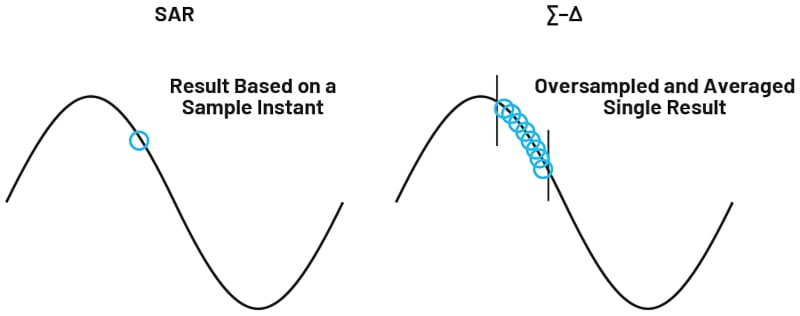
Figure 2. A SAR (ƒSAMPLE) vs. sigma-delta (ODR). Image used courtesy of Bodo’s Power Systems [PDF]
The first timing consideration for a signal chain is the time it takes to bias/excite the sensor and power up the signal chain. Voltage and current sources will have to turn on, sensors biased, and start-up time specifications considered. For example, the turn-on settling time for the AD4130-8 on-chip reference is 280 µs for a specific load capacitance on the reference pin. The on-chip bias voltage, which can excite sensors, has an associated start-up time of 3.7 µs per nF but depends on the amount of capacitance attached to the analog input pins.
After power-up times in the signal chain are investigated, we need to look at timing considerations that apply depending on the ADC architecture. We will begin the next section of the article by focusing on measurement signal chains with sigma-delta ADC at their core when used in ultra-low power applications and the important timing considerations associated with this type of ADC. There will be some overlap between SAR and sigma-delta signal chains that impact timing, such as using techniques that minimize the microcontroller interaction time to achieve system-level power consumption improvements. These will be highlighted when we move onto the SAR ADC signal chains.
Analog Front-End Timing Considerations
We will focus on the three blocks independently, starting with the analog front end (AFE). The AFE can vary depending on the type of design, but some common aspects can apply to most circuits.

Figure 3. The AFE sigma-delta timing considerations. Image used courtesy of Bodo’s Power Systems [PDF]
The AD4130-8 is part of the precision low-power group of signal chain products and is specifically designed with rich features set to reduce power while still achieving a high level of performance. These features include an on-board FIFO, a smart channel sequencer, and duty cycling.
The AD4130-8 is Analog Devices’ lowest power sigma-delta ADC. The ultralow current is impressive because it contains many key signal chain building blocks on the chip, such as an on-chip voltage reference, a programmable gain amplifier (PGA), a multiplexer, and a sensor excitation current or sensor bias voltage.
When we consider the AFE of this device, it consists of an on-chip PGA minimizing the analog input current, and this removes the need for external amplifiers to drive the inputs. Oversampling followed by a digital filter ensures that the digital filter dominates the bandwidth. The AD4130-8 offers several on-chip sinc3 and sinc4 filters and filters designed to reject 50 Hz and 60 Hz noise. The sinc3 and sinc4 digital filters require supplementary external antialiasing filters. The purpose of this antialiasing filter is to limit the amount of bandwidth of the input signal. This ensures that noise, for example, with a rate of change at fMOD (the modulator frequency), does not alias into the passband and the conversion result.

Figure 4. The AD4130 sigma-delta simplified system blocks. Image used courtesy of Bodo’s Power Systems [PDF]
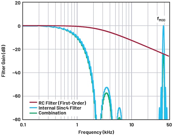
Figure 5. A simulation of combined external and internal filtering. Image used courtesy of Bodo’s Power Systems [PDF]
Antialiasing Filter
Higher-order antialiasing filters can be used, but first-order, singlepole, low-pass filters are typically used to satisfy requirements. Filters are designed based on sampling the signal of interest with Equation 1 dictating the filter 3 dB BW:
\[f_{3dB}=\frac{1}{2\times\pi\times RC}\,\,\,\,\,\,\,\,\,\,(1)\]
A higher resistance is more desirable when selecting the capacitor and resistance values. Still, it may increase noise while the lower capacitor values reach a limit, after which the ratio of the pin capacitance to the external capacitance becomes relevant.

Figure 6. A first-order low-pass antialiasing filter. Image used courtesy of Bodo’s Power Systems [PDF]
It is important to know the time it will take the circuit to charge based on the maximum voltage step that could be seen across this capacitor.
The voltage seen at the capacitor will change concerning time at a rate of change of
\[V_{C}=V_{S}\Bigg(1-e^{\Big(-\frac{t}{RC}\Big)}\Bigg)\,\,\,\,\,\,\,\,\,\,(2)\]
VC = voltage across the capacitor at a point in time
VS = Supply voltage applied; τ = Time
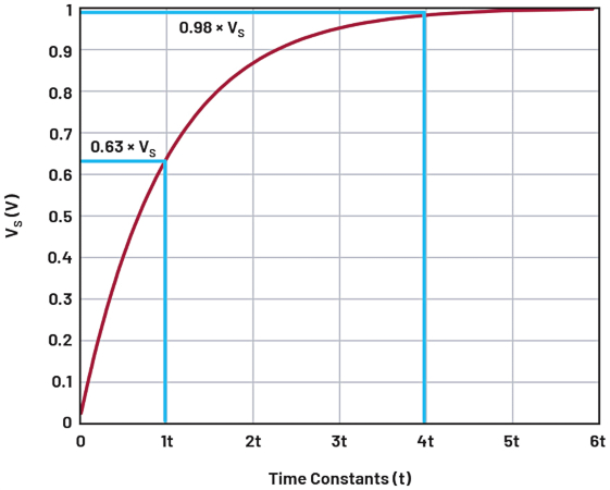
Figure 7. First-order low-pass filter settling time in response to a 1 V full-scale step change. Image used courtesy of Bodo’s Power Systems [PDF]
On power-up, VS, the step size could equal the full input voltage range of the ADC (±VREF/gain).
Figure 7 shows that after 4-time constants (τ = R × C) the signal has reached 0.98 × VS. The number of time constants required can be calculated from the natural logarithm of the ratio of the step size, VS.
\[N_{T}=ln\Bigg(\frac{V_{S}}{V_{HALF\_LSB}}\Bigg)\,\,\,\,\,\,\,\,\,\,(3)\]
NT is the number of time constants to wait for if the input is to settle to within half of an LSB (VHALF_LSB) of the ADCs’ input voltage span. The VHALF_LSB in the previous formula can be substituted based on the voltage accuracy required. If the system designer wishes to resolve to within half an LSB for a bipolar input ADC with N bits of resolution and with internal PGA gain = 1, this will be:
\[V_{HALF\_LSB}=\Bigg(\frac{2\times V_{REF}/Gain}{2^{N}+1}\Bigg)\,\,\,\,\,\,\,\,\,\,(4)\]
The time that it takes to resolve to the real input voltage tACQ becomes the number of time constants multiplied by τ, which is equal to RC:
\[t_{ACQ}=\tau\times N_{T}\,\,\,\,\,\,\,\,\,\,(5)\]
Traditionally, when switching between channels on multiplexed ADCs, a large voltage swing (one channel at negative full scale, the next channel at positive full scale) between channels would require a similar calculation. The AD4130-8 solves this problem by implementing a low-power on-chip precharge buffer that turns on when switching between channels. This ensures that the first conversion after switching channels will be converted correctly at the fastest data rates. There is also an on-chip PGA designed to allow a full common-mode input range, giving system designers a greater margin for widely varying common-mode voltages. This is useful for measuring signals, but in the worst case, one channel could be at a negative full scale, while the next channel could be at a positive full scale.
Example: Analog Front-End Low-Pass Filter
The example in Figure 8 shows a Wheatstone bridge sensor with a –3 dB filtering for a 24-bit ADC just below 16 kHz.
R = 1 kΩ, C = 0.01 µF with VREF = 2.5 V and the PGA gain set to 1:
The single-ended filters in Figure 8 show the primary sensor R = 1 kΩ and C = 0.01 µF:
\[\tau=10\mu s\,\,\,\,\,\,\,\,\,\,(6)\]
The differential signal filter in Figure 8 shows the primary sensor R = 1 kΩ and C = 0.1 µF. For more information on the formula, see MT-070:
\[\tau=50 \mu S(1k\Omega\times0.1\mu F/2\,\,\,\,\,\,\,\,\,\,(7)\\V_{HALF\_LSB}=298nV\]
As the differential sensor time constant dominates the single-ended values, it will dictate the overall system calculation:
\[N_{T}=16\tau(if\,V_{STEP}=5\,V)\,\,\,\,\,\,\,\,\,\,(8)\\t_{ACQ}=0.8ms\]
This is when a system designer would need to allow the filter to settle externally before gathering a sample on power-up. This can be done in the digital domain by discarding samples, or the sample instant can be delayed to account for this charge.
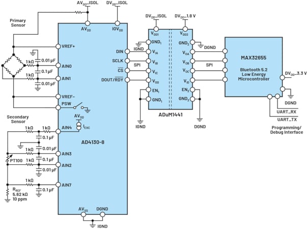
Figure 8. An isolated AD4130-8 circuit with a low-pass filter is shown. Image used courtesy of Bodo’s Power Systems [PDF]
When designing a filter, the resistor and capacitor values may differ from what is shown earlier. System designers can model the filter together with the AD4130-8 using LTspice. LTspice can also be used to model a system or signal chains, as shown in Figure 9, where we simulate an RTD behavior by varying R2.

Figure 9. A simulation of an RTD (R2) circuit in LTspice. Image used courtesy of Bodo’s Power Systems [PDF]
ADC Timing Considerations
Recalling that output data rates are how sigma-delta ADC timing is referred to, let’s examine the internal timing associated with this type of ADC.

Figure 10. The sigma-delta ADC timing considerations. Image used courtesy of Bodo’s Power Systems [PDF]
This type of converter digitizes an analog signal with a low-resolution (1-bit) ADC at a high sampling rate. By using oversampling techniques in conjunction with noise shaping and digital filtering, the effective resolution is increased.
An SPI written to a digital register allows users to control the oversampling and decimation rate of the AD4130-8. The modulator sample rate (fMOD) is fixed. The FS value essentially changes the number of samples (in increments of 16 for the AD4130-8) used by the digital filter to reach a result. Varying the FS word changes the number of oversampled modulation clocks per ADC result.

Figure 11. Decimation. Image used courtesy of Bodo’s Power Systems [PDF]
As decimation reduces the effective sampling rate at the ADC output, it achieves higher accuracy. Decimation can be viewed as the method by which the redundant signal information introduced by the oversampling process is removed. The more decimation used (the more samples included in the digital filter calculation), the more accuracy is achieved by the said digital filter, but the slower the output data rate.
\[f_{ADC}=\frac{f_{MOD}}{16\times FS}\,\,\,\,\,\,\,\,\,\,(9)\]
where:
fADC is the output data rate
fMOD is the mater clock frequency
FS is the multiplier used to control the decimation ratio
Filter Latency
When more than one channel is enabled, the link between the datasheet output data rate or ODR (fADC) and the data throughput rate is more complex. This is due to the latency of the digital filter when switching channels. The time the digital filters need to settle depends on the sinc filter type. Figure 12 shows that the first conversion of the sinc3 filter will take three conversion cycles until the digital equivalent to the analog input is reached. The first conversion of a sinc4 filter will take four conversion cycles. The tSETTLE is the user-programmable settle time that considers the mux switching. The higher the filter order, the lower the noise, but the downside is the number of conversion cycles needed for the filter to settle.
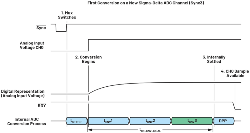
Figure 12. Filter latency. Image used courtesy of Bodo’s Power Systems [PDF]
Digital Interface Timing Considerations
To understand the digital interface timing in sigma-delta ADCs like the AD4130, a model is available via the ADI software tool ACE. The timing tools are part of several software tools integrated into the ACE software. There is a sequencer timing diagram and a FIFO timing diagram to aid in the understanding of these configurations.
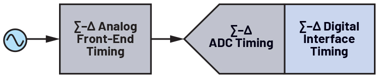
Figure 13. AFE sigma-delta digital interface timing considerations. Image used courtesy of Bodo’s Power Systems [PDF]
The AD4130-8 sequencer allows different input channels to have different digital filters, settling configurations, and timing. The timing tool simplifies calculating when data will be available to read.
When more than one channel is enabled, the user should not make the mistake of reading a settled channel ODR and dividing by the number of channels enabled to calculate the throughput rate because this does not consider digital filter latency. The filter latency should be considered when calculating the throughput rate (effective ODR vs. data sheet ODR). When more than one channel is enabled, the initial settling (tSETTLE) needs to be calculated, and the number of internal conversion cycles (t1st_CONV_IDEAL), as shown in Figure 14.
If all channels have the same filter plus settling configuration and there are no repeat conversions on any channels, the throughput rate of a system becomes:
\[Throughput\,Rate(SPS)=\frac{1}{(t_{1st\_CNV\_IDEAL+t_{SETTLE}})}\div CHS\,\,\,\,\,\,\,\,\,\,(10)\]
where:
CHs = is the number of channels enabled
t1ST_CNV_IDEAL = is the conversion time, including the filter latency
tSETTLE = a digitally controlled timing parameter that can be extended but with a minimum programmable time to account for the mux settling
The throughput rate can be calculated by looking at the sum of the 1CNV_ODR times, the time shown between the green squares in Figure 14.

Figure 14. The first conversion output data rate, including filter latency. Image used courtesy of Bodo’s Power Systems [PDF]
\[t_{1CNV\_ODR}=t_{1st\_CNV\_IDEAL+t_{SETTLE}}
\\Throughput\,Rate(SPS)=\frac{1}{(\sum t_{1CNV\_PDR})}\,\,\,\,\,\,\,\,\,\,(11)\]
Example: Pressure Sensor Signal Chain Timing
If we want to design a system with multiple pressure sensors, represented by the pressure sensors in Figure 15, accompanied by a temperature sensor, one must ask:
A: How many pressure sensors per AD4130-8 can be deployed in the system?
B: What resolution can we expect if the voltage output range from the pressure sensor is 3 mV/V?
C: If a line in the plant needs at least 14 bits of effective resolution to meet the dynamic range system demands, how many load cells form the system?

Figure 15. A simplified pressure sensor system block diagram. Image used courtesy of Bodo’s Power Systems [PDF]
Part A
Step 1: Choose the gain
AVDD = 1.8 V. REFIN+ to REFIN– = 1.8 V
The 1.8 V excitation of the load cell at 3 mV/V will lead to a 5.4 mV maximum output of each load cell.
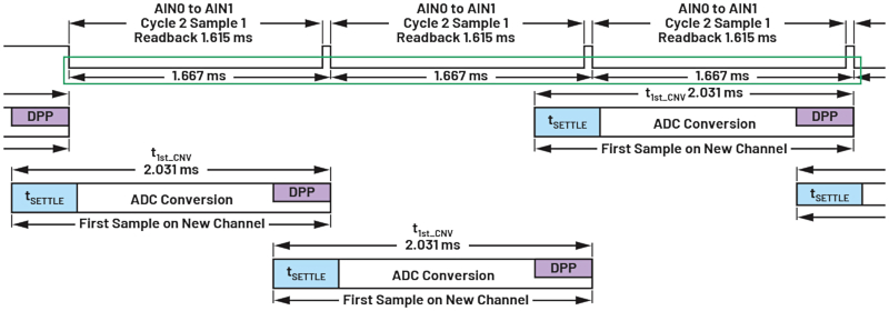
Figure 16. Calculating the sum of t1CNV_ODR using the timing tool. Image used courtesy of Bodo’s Power Systems [PDF]
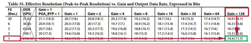
Figure 17. FS word vs. gain. Image used courtesy of Bodo’s Power Systems [PDF]
The maximum gain on the PGA = 128.
The ADC input will see 5.4 mV × 128 = 0.7 V across its inputs, well within the 1.8 V range. A PGA gain of 128 is the correct gain to use.
Step 2: Choose the FS value
We want to choose the fastest settings with a sinc3 filter and FS = 1.
Step 3: Use the throughput rate for one channel to calculate the number of channels in the system
1CNV_ODR = (1/1.667 ms) 600 SPS.
Throughput rate = 600 SPS/Nch.
1CNV_ODR = Throughput rate for a single channel in a multichannel system with the same configurations and no repeat conversions.
Ten channels can be sampled at 60 SPS.
Answer A: Nine load cells per system.
Step 4: Use the data sheet effective resolution tables
Another point to consider is that when looking at noise and effective resolution tables, the calculations must be based on the FS filter value, not the throughput rate. The ODR listed here is the settled channel ODR on a single channel.
System designers need to be careful when interpreting the data sheet. When more than one channel is enabled, the throughput rate in SPS decreases. There is a danger that readers might incorrectly interpret the resolution tables in the data sheet and think that a higher resolution is achievable. With settled channel ODR, the change in FS leads to an increase in oversampling and decimation, slowing down the system to achieve higher accuracy. When more than one channel is enabled, the decrease in the reading speed from each ADC channel in SPS (throughput) is due to sampling on more than one channel. An increase in oversampling does not cause it; hence, there is no increase in the resolution.

Figure 18. A resolution vs. gain datasheet table. Image used courtesy of Bodo’s Power Systems [PDF]
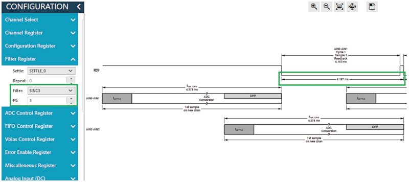
Figure 19. Using the timing tool to change the filter type and FS value and read the output data rate of the first conversion that includes filter latency. Image used courtesy of Bodo’s Power Systems [PDF]
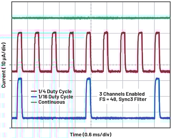
Figure 20. Duty cycling. Image used courtesy of Bodo’s Power Systems [PDF]
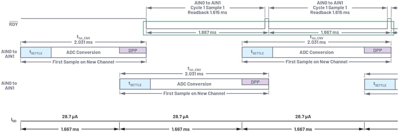
Figure 21. The throughput time and current before enabling duty cycling. Image used courtesy of Bodo’s Power Systems [PDF]

Figure 22. The throughput time and current after enabling duty cycling. Image used courtesy of Bodo’s Power Systems [PDF]
Part B
If we look at the table in the datasheet, we see that the effective resolution is 11.7 bits for FS = 1 and gain = 128.
Answer B: 11.7 bits.
Part C
To solve for C, we need to return to a couple of steps from Part A:
Step 2: Choose the FS value
This time, we choose the FS value based on the resolution requirement. To achieve an effective resolution of 14 bits, an FS of 3 should be selected.
Step 3: Use the throughput rate for one channel to calculate the number of channels in the system.
We can use the timing AFM to achieve the resolution needed (1/4.167 μs).
240 SPS/Nch = Throughput rate.
We can use four channels at this data rate.
Answer C: Three channels.
Duty Cycling
There are systems with lower throughput rates and higher output data rates, such as health monitoring devices, where the host controller puts the system in standby mode most of the time and converts periodically. Duty cycling is available on the AD4130-8, and this allows the user to continuously convert with the part entering standby mode for 3/4 or 15/16 of the duty cycle while the part converts for 1/4 or 1/16 of the duty cycle. Active time and standby time are functions of the settings chosen by the user.
The AD4130-8 also incorporates a SYNC pin that allows the user to determine when conversions occur on a preselected number of channels. The part can also be configured to work in a reduced current standby mode, initiate a conversion sequence, leave the reduced current state, convert on several channels, and return to standby mode when the conversions have been completed.
Example: Enabling Duty Cycling
Taking the same settings as the previous pressure sensor signal chain example and the throughput rate = 600 SPS/Nch, enabling two channels, the ODR becomes 300 SPS while the average current would be 28.7 µA on average with a 3 V supply (see Figure 21).
After enabling duty cycling 1/16, the throughput rate becomes 24.489 SPS while the average current becomes 4.088 µA over that period (40.834 ms; see Figure 22).
FIFO
The AD4130-8 includes an on-board FIFO. A FIFO reduces system power by buffering the conversions and allowing a microcontroller or host controller to enter a low-power state while waiting for conversions. The biggest timing consideration here is to ensure the host reads back the FIFO quickly enough while continuously converting to avoid missed conversions.
The user can periodically read the FIFO when a specified number of samples (a watermark) has been gathered. An interrupt is available when a desired number of samples is reached, and the host reads back the FIFO. The FIFO needs to be emptied to clear the interrupt. The user has a predefined period to read back data from the FIFO. The SCLK frequency will determine how much data one can read without missing conversions.
The ACE software timing tool allows the user to vary the SCLK frequency or use a gated clock to inform the user when they need to reduce their watermark level while designing their system. For example, the FIFO readback.
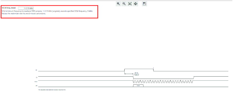
Figure 23. The AD4130-8 ACE software FIFO readback window and alert. Image used courtesy of Bodo’s Power Systems [PDF]
Take the example of a continuous single-channel measurement running at the maximum ODR of 2400 kSPS. If the watermark level is set to 256 and we attempt to read back, we have 729.2 µs to read back the FIFO without missing a conversion. The user needs to read back 4112 bits. The tool informs the user that to read the FIFO back and not miss a conversion, 5.64 MHz of a host SPI clock frequency is needed. This breaks the 5 MHz maximum specification for the part, and an error appears, allowing the user to modify their watermark to avoid breaking the specification.
Table 3. Sigma-Delta Summary
| Topic | Timing Impact | Low-Power Signal Chain Impact |
| Signal Chain PowerUp | Delays powering up each block | Applies to all signal chains |
| Antialias Filtering | Delays can exist that impact the conversion result(s) | AD4130-8 precharges filter when switching channels |
| Sinc Filter Latency | Throughput rates on multiplexed systems are impacted | Multiplexing allows for improved power savings (µA/ Ch) |
| Duty Cycling | Throughput rates are reduced while duty cycling | Average current decreases proportionally |
| FIFO | Care is needed to avoid missed conversions | Host controller can enter a low-power state |
When a sigma-delta ADC is used, we can see plenty of trade-offs, timing factors, and features to consider. Part 2 of this series will examine the SAR ADC technology and the factors and features that impact timing in SAR ADC-based systems.
This article originally appeared in Bodo’s Power Systems [PDF] magazine.