 Facebook
 Google
 GitHub
 Linkedin
Intelligent Power Amplifier Module Based on GaN FETs
Due to their outstanding characteristics, GaN FETs play an increasingly important role in miniaturization of the switching converters with very high power densities
In the past few years, gallium-nitride (GaN) FETs have become more widespread in power electronics. Due to their outstanding characteristics, GaN FETs play an increasingly important role in miniaturization of the switching converters with very high power densities exceeding 100 W / cm3 and more.

Figure 1: Enhancement-Mode GaN Power Transistor from Efficient Power Conversion (EPC)
The efficiency of converters based on GaN transistors can reach 99.5%. Due to the expansion of the conversion frequency range towards the MHz, the magnetic components (chokes, transformers) also decrease in size significantly. However, designers face numerous challenges in implementing practical GaN transistor designs. The best family members are presented in wafer-level chip-scale package; the drivers are also quite miniature. There is a significant problem in optimizing the gate control circuit and its topology due to enormous switching speed. Reminder, GaN FETs have no familiar parasitic body diodes which affects the application design. Taking into account the values of the currents and voltages relative to the size of the power elements, it becomes clear that a new design approach is needed in terms of the PCB topology, heat dissipation and ensuring the safe area operation for all working modes. As usual, the designer must choose 2 of 3 between "Cost", "Efficiency" and "EMC", but for GaN FETs this combination is extended compared to Si MOSFETs.
To simplify and accelerate the development process of many devices (D-class audio amplifiers, AC current and voltage calibrators, power supply modulators etc.), the idea of creating an Intellectual Power Amplifier Module (IPAM) with the following parameters appeared:
- Supply voltage up to 80 V, output current up to 20 A
- Sinusoidal output power 500 watts
- Efficiency 98% (half power), 96% (rated power)
- Full Power Bandwidth 0…50 kHz
- Main carrier frequency 1 MHz, internal transitions up to 10 MHz
- Less than 0.01% THD (-1dB)
- Diagnostics and parameter setting via 2-Wire Serial Interface (TWI)
IPAM is a fully differential pulsing power amplifier covered by a common negative feedback. Typical carrier frequency is approximately 1 MHz and may vary within ±50 % based on input level, output power and load impedance. A high-speed precision comparator is used as an error amplifier.

Figure 2: Functional Block Diagram
The module contains small FPGA chip. The first important FPGA function is to produce additional pulses for the best amplifier linearity. The second FPGA function is to maintain safe operating modes of the power switches and the output choke, regardless of the parameters of the input analog or PWM signal. FPGA limits the modulation index and some other parameters. When the transition frequency drops below the limit, the FPGA generates extra pulses that prevent the UVLO detector from triggering due to the discharge of bootstrap capacitors. The minimum pulse length is also limited to comply the driver circuit possibilities. If the parameters of the input signal correspond with the introduced restrictions, the pulse sequence from error amplifier output is transmitted asynchronously to the half-bridge drivers, with a delay of less than 5 ns and minimal time distortion. All parameters are programmable via TWI and can be deactivated by user.
IPAM has no dependency on THD+N vs Frequency and has very low dependency on THD+N vs Output Power thanks to its original control loop structure. For output power up to 200-250 W RMS, IPAM does not require an additional heatsink for generic scenarios.

Figure 3: THD+N vs Frequency, VPWR=48 V, RL=4 Ohm, POUT=100 W
The problem of heat removal is solved by a complex way. A 6-layer PCB with 35 μm Cu on the outer layers and 70 μm on the inner layers is used, vias are filled with copper. The module is housed in CNC machined aluminum enclosure with 76 x 36 x 18 mm dimensions. At the last stage, vacuum filling is performed with a specialized ceramicbased compound with very high thermal conductivity.

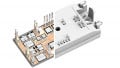
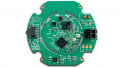
Figure 4: Pre-production samples
The development of the output choke has turned into a separate R&D work related to the need to study the parameters of the newest high-frequency power ferrites manufactured by TDK/Epcos and Ferroxcube. Unfortunately, these companies did not provide sufficient data for accurate calculations. I had to find a way to make samples with different gaps and different numbers of turns and study them in details. It took more than one month with the corresponding costs.
As a result, 33 μH small-sized chokes with a 20 A linear current range and SRF > 10 MHz were created. Unfortunately, the world industry does not produce chokes with similar characteristics. I’ve got about 16 usable chokes with different parameters.
I also had to study the real characteristics of various film capacitors for the output demodulating LC filter and opt for products with a polyphenyl sulfide dielectric. Ceramic capacitors are not suitable for these purposes due to their enormous nonlinearity. The special attention was paid to choose optimal ceramic blocking capacitors for the power stage. I'm not sure if I could do this work without Vector Network Analyzer, 2 GHz Oscilloscope with active probes and a couple of burning experiments at the start. Many reference designs are "thing in itself" and can work only “as is” on your lab table but doesn’t work in real environment, especially if they are tied up by external connections which produces EMI problems. I managed to achieve that almost all high-frequency components of the switching current circulate inside the module.
Please carefully design the gate driver circuit, if you want to save high efficiency and don’t want to have EMI problems in the future. I highly recommend to simulate the circuit adding parasitic inductances before you start to burn it naturally. With GaN FETs, there is a very thin trade-off between the reliable gate control and practical parameters (Efficiency, EMI). The classic way to simply increase or decrease the gate resistor is not suitable for many cases due to the risk of GaN FETs unexpected behavior. It is possible to find the way how to keep confident control of the gate. I propose to use several wonderful properties of ferrite beads which can be used for some non-trivial cases.
Due to the extremely high dV/dt and dI/dt significant voltage spikes occur between the power and signal grounds of the module during operation. I added galvanic isolation for TWI and ERR/ENA control signals.
The RGB LED indicates the fact and cause of multiple failures. The types of errors are encoded in series of flashes separated by a long pause. IPAM can be re-initialized automatically, using the built-in timer that generates the protective interval.
A general purpose 2-phase module without an output demodulating filter is under development. It can be used for a wide range of DC/DC converters with different topologies (buck-, boost- or LLC). 3-phase version of the power module with similar parameters can be built.
I met big logistics problems throughout the crazy 2020 year, as well as big lies from some component suppliers. In particular I had to abandon the GaN-drivers from one manufacturer and start over again completely with another driver IC because the first prototypes burned out like candles for inexplicable reasons. In the end this manufacturer set NRND status for these ICs continuing to ignore my mails.
I would like to express my gratitude to EPC European office for the timely support. The result of this big two years’ work is a deep understanding of the capabilities of GaN power electronics. A number of architectural, circuitry, topological and design solutions have been developed, which now make it possible to develop a wide range of various devices for breakthrough electronic systems.
References:
- https://epc-co.com/epc/GalliumNitride/whygan.aspx
- https://patents.google.com/patent/US20110068864A1/en
- https://www.ti.com/lit/wp/slyy085/slyy085.pdf
- https://epc-co.com/epc/Portals/0/epc/documents/papers/eGaN FET Electrical Characteristics.pdf
This article originally appeared in Bodo’s Power Systems magazine.
About the Author
Pavel Gurev worked at Sinftech Rus LLC.


Hi. Our company is Eta Research Ltd., a high-tech company set up in Shanghai in April 2015. We focuses on growing large size high-quality GaN wafers which can be produced for an affordable price for semiconductor industries, and has adopted self-developed HVPE as the production method for GaN wafers. If you are interested in our product, you may search our official website http://www.etaresearch.com/ for more information or mail to .(JavaScript must be enabled to view this email address).
It will be a great pleasure to receive your inquiries for any of the items against which we will send you our competitive price with high quality.