Facebook
 Google
 GitHub
 Linkedin
Acoustic Modes for Full-Depth Component Imaging
When a pulse of ultrasound is fired from an Acoustic Micro Imaging system’s transducer into a component, the pulse will be both reflected by and transmitted through any solid-to-solid interfaces that it strikes before its energy is exhausted. Around this simple event, more than a dozen different acoustic imaging modes have been designed.
Multiple modes are possible because the echoes returned by the pulse contain four types of information (amplitude, travel time, frequency and polarity).
The most frequently used imaging mode is the C-Scan imaging mode, also known simply as Reflection Mode. Echoes are received from ultrasound pulsed into a component, and the arrival time and amplitude of echoes returning from a defined depth are used to make the acoustic image. Each amplitude is given its own grey tone or color. In a plastic-encapsulated integrated circuit, for example, all bonded interfaces between mold compound and silicon may be light blue. Reflection Mode has one inherent limitation: it may be difficult to bring the entire thickness of a component into focus.
The component’s image is made by the moving transducer which launches the pulses and then collects and assigns colors to the echoes arriving from tens of thousands of x-y locations per second. The completed image will show all the features within the gated depth. “Gated” means the time, measured in microseconds, after the launch during which the transducer has been programmed to receive return echoes. Gates may be long or short, and there may be multiple gates, probably sequential, to image, for example, a vertical sequence of interfaces in order to be able to view separately each depth of the component. With the right imaging mode, however, it is also possible to scan the entire thickness of the component and image all features, including defects, without significant loss of focus. In the Nordson SONOSCAN C-SAM™ Acoustic Micro Imaging tools, two different modes can perform this task: THRUScan™ and Loss of Back Echo™ (LoBE). In neither of these modes is maximum resolution as sharp as in the most in-focus depth in a Reflection Mode image, but with the right transducer resolution is relatively consistent throughout the thickness of the component.

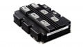
Figure 1. Optical photo of the IGBT module discussed here. Image used courtesy of Bodo’s Power Systems
An optical image of the IGBT module discussed in this article is shown in Figure 1. The module has been turned upside down to show the heat sink through which ultrasound was pulsed for acoustic imaging. The white marks are surface scratches. In this posture, the features below the heat sink are the solder, the ceramic raft, and the die. There is no encapsulant on top of the die in this IGBT module. If there were, imaging with THRU-Scan might be possible, but only if the encapsulant was not so lossy that the pulse would arrive at the second transducer too weak to permit imaging. In that case, imaging would be through the heat sink, which has no impediments.

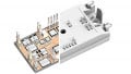
Figure 2. Side view diagram, not to scale, of layers in the IGBT module discussed here. Image used courtesy of Bodo’s Power Systems
A diagrammatic side view section through the raft is shown in Figure 2. Since the module has been inverted, the heat sink is at the top, as it is in Figure 1. The various layers of course have different thicknesses; the purpose here is only to identify the layers and show their vertical distribution. Note that THRU-Scan uses two transducers, one above and one below the component. LoBE uses a single transducer, but in a novel way.

Figure 3. Acoustic image of the whole module shows warping of the raft. Image used courtesy of Bodo’s Power Systems
A Reflection Mode image of the whole module is shown in Figure 3. The image is gated on the interface between the substrate and the raft, and reveals echoes for imaging only from this interface. The curved features identify warping in the ceramic raft.
The die lie beyond the raft and above this gate, and are not imaged here. The three substrates that comprise the module each hold four die. There is no encapsulant above the die. The acoustic images in this article were made using a Nordson SONOSCAN CSAM® Acoustic Micro Imaging tool.
THRU-Scan Imaging Mode
In THRU-Scan, as in most of the dozen or so other imaging modes, the transducer scans back and forth above the component (or tray of components). As it travels, it launches tens of thousands of pulses per second, receiving the echoes from each pulse before the next pulse is launched.
Unlike other modes, the sending transducer used in THRU-Scan launches the ultrasonic pulse but does not collect the return echoes, as is shown in Figure 2. The launched pulse travels through the whole thickness of the component, and is modified as it passes through each material interface. Reflected echoes reach the transducer that launched them, but the transducer ignores them.
The remaining energy of the original pulse proceeds downward and is collected by a second transducer placed below the heat sink on the bottom side the component.
For each of the many thousands of x-y locations, only the ultrasound exiting the bottom of the component is used to make the THRU-Scan image. The two transducers are mounted on a C-shaped bracket (not shown in the diagram) to ensure that they are always perfectly aligned with each other on the same x-y location as they scan the sample.
THRU-Scan can be used only where a transducer can access both sides of a component. Encapsulated IGBTs, for example, may not be suitable for imaging by THRU-Scan because of excess attenuation in the encapsulant, but are easily imaged by LoBE. The ultrasonic frequencies that may be used to image IGBT modules range from 10 MHz to 50 MHz. Overall, imaging frequencies range up to 300 MHz, but the higher frequencies lack the penetration needed for thicker components. Lower frequencies also have lower spatial resolution, with the result that THRU-Scan images, although comprehensive in their vertical coverage of the component, are able to image gap-type defects and other internal features. They do not, however, provide the fine details that a reflection mode image would give. The main purpose of THRU-Scan is to identify internal air gaps - voids, delaminations, cracks and the like anywhere throughout the thickness of the device. The method is successful because the solid-to-air interface of the defects reflects virtually all of the pulse. None of the pulses are transmitted through the air to the receiving transducer below, so it too records ”no signal” from this x-y location. The overall result: gap-type defects at any x-y location and at any z depth in the component will appear black in the THRU-Scan image.

Figure 4. THRU-Scan image of the leftmost section of the module seen in Figures 1 and 3. Image used courtesy of Bodo’s Power Systems
Figure 4 is the THRU-Scan image of the leftmost substrate in Figure 1. A low acoustic frequency of 20 MHz was used to be able to penetrate the five layers of material.
The circle at the center of each of the larger die, along with the horizontal line running through the circle, is a structural feature on top of the die. The black circle near the top of the image is a solder bump. The numerous faint forms faintly visible in the area of each die represent local modest variations in amplitude acquired by the arriving echo as it traveled through the component. The three similar oval features at the edges of the die are part of the metallization the ceramic raft.
Black features in the area of each die are air-filled voids. The solid-to-air interface in each air gap completely blocks the arriving pulse and prevents it from reaching the transducer below. The largest void is in the upper right die, but there are numerous smaller voids, mostly near the edge of a die. Air gaps - voids, delaminations, cracks, etc. - are frequent initiators of structural alterations that cause electrical failure.
Loss of Back Echo Imaging Mode
Loss of Back Echo (LoBE) begins much like reflection mode imaging: the transducer launches a pulse into a specific x-y location on the top surface of the component. The pulse sails through the few mm of water linking it to the component and sends back part of its energy as an echo. Within the component, the mildly diminished pulse encounters the first solid-to-solid material interface at that x-y location and again reflects part of its energy back toward the transducer, where the arrival of this echo is - ignored.
LoBE is interested only in those echoes reflected by the back wall of the component. All echoes that are reflected from higher levels will arrive before the time gate opens for back wall echoes and will not be recorded. (In some situations, it may be beneficial to open the gate a bit wider.) In Figure 2, the echoes reflected by the final interface are colored gray. The pulses will be diminished in amplitude by each material interface they encounter on the path to the back wall. Each echo reflected by the back wall will return along the same path, and will be attenuated again by the same interfaces it encountered on the way down, but in reverse order. Echoes received at the transducer in various x-y locations will therefore differ in amplitude and therefore in color, and the whole image will depict in detail each of the features that subtracted energy from the echo returning from the back wall. Intended features will be visible but so will air gap defects which have, on their top side, a solid-to-air interface that ultrasound cannot penetrate.

Figure 5. Loss of Back Echo (LoBE) image of the same section. Image used courtesy of Bodo’s Power Systems
Figure 5 is the LoBE image of the same IGBT module. No echoes are collected during the pulses’ downward trip. The only echoes to be collected are those reflected by the back wall.
The large void in the second die in the upper row, black in the THRU-Scan image, is bright here because the LoBE image is combined with the reflection mode image. A few other voids are large enough to have a pale center. But there are several smaller voids, mostly along the sides of the die, which are significant because thermal and mechanical forces can cause them to grow in various ways.
The bottom pair of die in each section have in their lower regions a curved white background that strongly suggests that the ceramic raft below is warped or tilted, as suggested in Figure 3. The white regions are probably higher than surrounding regions. They contain features in their brighter portions that are similar to the features seen in the THRU-Scan images. The one at the bottom right, for example, has a central small circle through which a horizontal line runs. It appears that warping has pushed some features of the substrate upward into the gate used for LoBE.
When a vertically comprehensive view of internal structure is needed, THRU-Scan or LoBE may be good choices. They both give the advantage of providing uniform spatial resolution to all depths within the component, thereby providing a view that cannot be achieved by gating echoes on selected depths. Both modes easily display pulse-blocking air gaps; LoBE is especially good at imaging thin, vertical cracks that other modes might miss. Choosing which of the two modes to use on a particular IGBT module often depends on the module's structure. If the module has an encapsulant on top of the die, THRU-Scan may work. But if the encapsulant attenuates too much ultrasound, the pulses may not arrive at the receiving transducer with sufficient strength. In that case, LoBE is the better choice.
This article originally appeared in Bodo’s Power Systems magazine.