Facebook
 Google
 GitHub
 Linkedin
High Power Density Dual nHPD2 Packaging Generation
This article introduces Hitachi's nHPD2 and its benefits in terms of market potential, performance, modularity and ease of transition.
The challenges of continuous improvement, for ever higher efficiency, reach far and wide within the Power Semiconductor industry – the engine of the modern world striving to achieve a more sustainable future. Semiconductor manufacturers and system designers alike tirelessly challenge the force that is the laws of physics. Worldwide Research & Development activity stretches daily from the simple to the complex in an effort to bring to market revolutionary ideas with a common goal. Working with a new fresh approach to product packaging and in an effort to achieve global standardization, Hitachi Limited outlines the Next High Power Density Dual or nHPD2, milestones and open source concept.
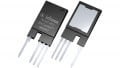
HITACHI has been contributing to the global power conversion industry through the continuous development of its High Voltage IGBT product family. Confined to existing IHM mechanical outlines, the latest HITACHI F-version chip generation could bring major benefits for efficiency improvements; in some cases 20% improvement in headline performance figures, but more is possible. nHPD2 from HITACHI is introduced to the market as the next de-facto, open-source, license-free external package standard.
Pressure on the converter and inverter markets can be felt throughout the supply chain with market forces demanding a Moore’s Law desire for more. More efficiency. More competitiveness. More compact solutions. With strong customer relationships, teamwork, collaboration and cooperation and that single goal for more can always be reached.
Of course, improved silicon designs are the usual first stop and a valid option. Conference subject matter and roadmaps around the world show on-going promise. New wide band gap technology (WBG), such as Silicon Carbide (SiC) or Gallium Nitride (GaN), have been hot topics for several years already and global manufacturers, including HITACHI, have made impressive new product announcements realized with WBG technologies. So where is the “but”? The fundamental advantages of these technologies, especially WBG, are often presented at the chip level. Step back and look at the impact at a system level and present-day IHM technologies struggle to bring out the best net performance gains. Ringing or oscillations [Figure 1(b)]; overvoltage spikes; high dv/dt; electromagnetic interference; and eventually the total expected gains begin to wane as countermeasures are applied to meet project specification limits and other application conditions. In the case of a traction drive system, motor winding insulation may be limited to 4-6kV/µs for example, so a high-speed switching device reaching 10kV/µs must be controlled, slowing the turn-on or turn_off, which pushes up losses. To highlight the potential increase of dv/dt during diode recovery, Figure 1 compares a 3.3kV silicon diode with a SiC diode using an existing 130mm x 140mm IHM packaging. Without sufficient mitigation oscillation appears as dv/dt increases from 30.0kV/µs to 40.0kV/µs due to SiC diode behaviour.

Figure 1: Comparison of Si vs. SiC recovery in IHM package, Lo=400nH, Tj=25°C. K. Ogawa, et al. “Traction inverter that applied SiC Hybrid module”, PCIM 2011
nHPD2 is a ‘clean sheet’ or ‘white paper’ design first, drafted by HITACHI in early 2013 to address the pending issues of how to get more useable power for less. Not only more useable output power from existing mature silicon (Si) but notably new generation SiC materials. The package design should not penalize those not participating in WBG and should bring merits to both material technologies.
The next-generation housing concept should at least meet existing power densities offered by IHM but at the same time bring a performance advantage. The package should offer global consumers of power semiconductors standardization, choice and competition. An open-source approach was a prerequisite to allow competition and innovation to directly benefit to wider market. Consumers and manufacturers setting a common goal: a new de-facto housing standard; a package standard that the market wants to consume because it meets common goals and benefits across a multitude of applications and technologies. A core principal of the open-source idea was to avoid setting a standard according to the single highest consumer at a specific moment in time.
Achieving less than 10nH internal inductance
Critical to future switching devices is low inductance. Enhancements to contemporary IHM package technologies through thorough simulation and internal layout structures featured heavily in the development cycle.
Inverter development engineers continually challenge trade-offs during the development cycle of their designs. One of the foremost obvious trade-offs at switching component level is gate resistor (Rg) selection versus system loop inductance.
Figure 2 shows the influence of Rg on IGBT turn-on loss plus diode recovery loss, where low Rg achieves the highest calculated efficiency. In conventional IHM modules, oscillation can only be avoided only by increased Rg which generates higher turn-on losses. However, using nHPD2 with its inherently lower package inductance the design engineer can maintain use of lower Rg values without oscillation and thus keep the total losses lower. It is important to avoid simple datasheet comparison of module stray inductance without consideration of resultant oscillation. Rg values must be kept higher for IHM to comply with relevant EMI regulations.

Figure 2: Loop inductance & gate resistor trade-off
Reducing system stray inductance can also eliminate oscillations, as can better driving algorithms, but there will be an impact on the system cost or increased losses of the driver negating their effect. Considering the switching characteristics of SiC with zero recovery losses, ringing becomes more of a menace. It is important to remember total losses and not focus on a single characteristics benefit, like low Eon for example. Higher inductance with low Rg will reduce Eon, however factoring in the oscillation loss, total losses will become significantly higher too. Careful selection of package inductance and Rg yields better net power losses, i.e. higher efficiency.
Layout
Featuring a P and N terminal pair on one of the short sides and the AC terminal at the opposite side nHPD2 provides design advantages and user convenience. Connection to sub-systems and components is made simpler by separating DC and AC lines. This offers the user the convenience to adopt more compact inverter designs by optimal DC-link capacitor and load connections. See Figure 3.

Figure 3 – Single-phase realized with two parallel nHPD2 LV450 modules
The dual switch concept is an important criterion to realize a 75% reduction of each phase leg, traditionally realized in high power applications using two series-connected devices as in Figure 4.
Standardization of the footprint dimensions in both low voltage (LV) and high voltage (HV) allows common heat-sink designs to keep non-recurring engineering design costs down as well as offering efficient production and material handling process. Combining wide a Voltage Class range in a common footprint, simply adding additional modules in parallel to increase output power, further enhances cost-competitive designs allowing for a higher number of common parts. Stock, production assembly processes and after-market service can all be streamlined to add further cost benefits.

Figure 4 – Single-phase realized with MBN1000E33E2
An inductance comparison is summarized in Figure 5. The left side features a traditional solution using two single IHM packaged 800A or 1000A IGBT modules, each with a stray inductance of 18nH (or 10nH for Hitachi’s latest F-version series). As a phase leg, the total phase inductance is 36nH. On the right is nHPD2 with a low 10nH module stray inductance value, has an equivalent inductance of only 5nH (10nH/2), a significant 75% lower, due to terminal optimization, dual topology and a modular parallel connection approach necessary to achieve the equivalent usable Current (A) performance of the IHM configuration.
Additional design effort for optimal internal terminal structure ensures balanced currents without negative effects or de-rating safe operating areas of the upper and lower side switches as well as reduced terminal resistance to improve laminate bus-bar connection thermal stress.
External positioning of P and N terminals, as well as P-N to AC terminals, is carefully considered to minimize the module stray inductance, mitigating potential ill-effects of final external bus-bar connections, maintaining sufficient creepage and clearance distances, whilst leaving a reasonable area [6000mm2] on the upper side of the nHPD2 package for direct mounting of a full or final stage gate driver via up to four dedicated fixed mounting positions.
Working with the modular nHPD2 design concept, up to five (LV or HV) modules may be connected in parallel without de-rating to achieve or exceed the latest single package Current (A) ratings. Considering the ultra-low nHPD2 stray inductance at a system level, it is easily achievable to realize an improvement of 60% system stray inductance versus conventional IHM packages at inverter level allowing for the capacitor DC-link.
Without such aggressive efforts to improve package stray inductance improvements, WBG technology benefits will simply be wasted.

Figure 5 – Phase leg inductance of IHM vs. nHPD2
Modular. Scalable. Convenience.
nHPD2 is a modular concept. It is designed with paralleling in mind and a common package for a wide range of Voltage classes. This modular and scalable concept offers the consumer significant direct cost benefits. To achieve an inverter product line-up, clients must currently qualify a range of HV-IGBTs. Although the internal semiconductor switches and diodes may be common, due to the Ampere ratings being split between three common footprints, qualification efforts and direct non-recurring engineering charges can be triplicated to offer the end-user's market a broad range of inverter power levels within budget and versus market prices. Efforts to realize an inverter family may be further cost impacted by Voltage class. Raising the Voltage level may require a totally different package solution, especially from 1200V to Š1700V or 3300V to Š4500V.
For new “white sheet” inverter series development, qualification of existing IHM HV-IGBT modules requires procurement of several samples and the resources to test several modules. This takes time, money and huge effort.
Understanding this gap in clients’ needs and the inconvenience of changes in Current and Voltage to mechanical designs, the nHPD2 scalable package concept offers major convenience. A truly common footprint from 1200V-6500V, split into only two housing types: LV (1200V-3300V) and HV (3300V-6500V), necessary to achieve regulatory requirements, for example creepage and clearance.
If the user requires more output Current simply parallel additional nHPD2 modules. If a higher Voltage capability is required heat-sinks may be re-used bringing significant cost savings. All that may be required would be to validate the new higher Voltage class chip characteristics.
High power density
Usable power might be questioned at this stage. nHPD2 is afterall smaller than the mid-sized IHM footprint at a compact 94mm x
140mm. However, this is not at the expense of a reduction in usable power. nHPD2 is a high power density dual. Powered by Hitachi’s latest F-version chip series and utilizing the stray inductance benefits, the usable power is in fact increase of almost 10% versus.
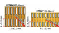
Considering the phase leg [Figure 5] and comparing (i) MBN1200F33F vs. (ii) LV450, we may calculate comparative total power densities according to respective Rth(j-a) specifications:
1200A x 2 / (135 x 285) = 0.0623A/mm2
450A x 2 x 2 / (188 x 140) = 0.0684A/mm2
Therefore, nHPD2 guarantees to offer a better power density performance in a 2-level inverter than an equivalently rated IHM module.
Gate drive
Gate drive design has been considered during the development process via consultation. According to 3rd party feedback from client in-house gate drive design teams and off-the-shelf vendors, varying levels of integration are possible, from simple final MOS drive with limited clamp protection discretes, to a highly integrated full driver are possible within the available mounting area provided.
Package tolerances and the ability to mount parallel modules side-by-side, the nHPD2 package ensures sufficiently tight tolerances for the GDU PCB to span up to five parallel modules. Four integrated fixed mounting positions ensure a durable connection allowing mounting
of the inverter in any axis without suffering ill-effects of relevant IEC shock and vibration test conditions. Additional fixed auxiliary terminals enhance mounting security accommodate drivers up to 250 grams (per module).
Conclusion
nHPD2 offers the market high-performance potential from existing switching technology and next-generation WBG devices alike. Advanced simulation techniques, a clear “system level, not device level” design brief and a pure open-source approach will all combine to give more without compromise. Modularity and footprint standardization from 1200V-6500V. 75% lower inductance. Up to 10% better power density (versus IHM). A future proof package concept accommodating new wide band gap semiconductor technology to ease upcoming transitions from silicon-based designs without mechanical changes. Samples for nHPD2 are available to order via Hitachi Europe Limited from November 2014. Launch products will be rated 900A 1700V (LV900) and 450A 3300V (LV450). 225A 6500V (HV225) to follow.
For other manufacturers, please contact directly and ask for their nHPD2 availability schedules. nHPD2 is an open-source, license-free HITACHI technology standard.
About the Authors
Neil Markham works as the Product Marketing Manager of Power Devices Division at Hitachi Europe Lt., a European branch of the highly diversified Japanese company, Hitachi Ltd., that operates eleven business segments: Information & Telecommunication Systems, Social Infrastructure, High Functional Materials & Components, Financial Services, Power Systems, Electronic Systems & Equipment, Automotive Systems, Railway & Urban Systems, Digital Media & Consumer Products, Construction Machinery and Other Components & Systems.
Katsuaki Saito works at Hitachi as an STA at Hitachi Europe Ltd, a European branch of the highly diversified Japanese company, Hitachi Ltd., that operates eleven business segments: Information & Telecommunication Systems, Social Infrastructure, High Functional Materials & Components, Financial Services, Power Systems, Electronic Systems & Equipment, Automotive Systems, Railway & Urban Systems, Digital Media & Consumer Products, Construction Machinery and Other Components & Systems.
Related Content