Facebook
 Google
 GitHub
 Linkedin
Generating Very Low Voltages with Standard Regulators
Question: What is a good solution for generating a tiny dc supply voltage of a few hundred millivolts? Answer: All that is needed is a clean additional positive voltage to hook up to the feedback resistor of a dc-to-dc converter. Supply voltages for electronic components have been decreasing steadily over the last few years. The reason for this is the decreasing size of the geometrical structures in digital circuits such as microcontrollers, CPUs, DSPs, and others.
There are also applications in the measurement field that require low supply voltages. For many years, linear regulators and switching regulators had a feedback voltage of approximately 1.2 V. This voltage was generated with a band gap circuit in a dc-to-dc converter IC, which determined the lowest voltage that could be set with an external resistive divider. By now, most modern voltage regulator ICs can generate output voltages of 0.8 V, 0.6 V, or even 0.5 V. The internal voltage reference is designed in such a way that lower voltages are possible. Figure 1 shows such a switching regulator, the LTC3822, which generates a feedback voltage of 0.6 V with a 0.6 V voltage reference.
Image used courtesy of Bodo’s Power Systems
However, if a supply voltage of less than 0.6 V is required, the circuit in Figure 1 cannot be used without further adjustments.
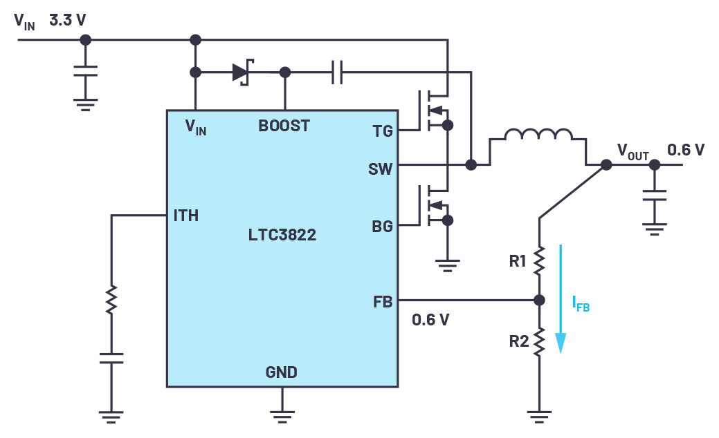
Figure 1. An LTC3822 dc-to-dc converter for generating low output voltages of 0.6 V or higher. Image used courtesy of Bodo’s Power Systems
With a trick, you can make a switching or linear regulator also generate lower voltages than the feedback voltage. This can be achieved by using circuits like the one shown in Figure 2. It requires an additional positive supply voltage to which the resistive divider is connected for adjustment of the output voltage. This voltage can come from a low dropout (LDO) regulator or a voltage reference. The resistive divider thus forms a voltage divider in which the current flow IFB flows in a direction opposite to the normal case in Figure 1. In Figure 2, the current flows from the external reference voltage through the resistive divider to the output voltage.
Equation 1 shows the relationship between the feedback voltage of the IC (VFB), the desired output voltage (VOUT), the additional positive dc bias voltage (VOFFSET), and the resistors of the resistive divider R1 and R2.
\[\frac{V_{FB}-V_{OUT}}{V_{OFFSET}-V_{OUT}}=\frac{R1}{R1+R2}\]
The recommended values for the resistive divider are a total value of R1 plus R2 of between 100 kΩ and 500 kΩ. This keeps the bias current low enough in regard to power efficiency but high enough to prevent from excessive noise coupling into the sensitive feedback path.
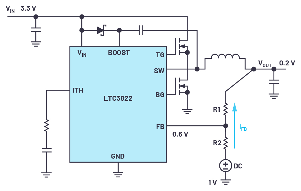
Figure 2. Circuit of Figure 1 was modified to generate output voltages of less than 0.6 V. Image used courtesy of Bodo’s Power Systems
This concept generally works well for generating voltages below the specified minimum voltage of a switching regulator or linear regulator. However, a few things should be considered. The additional voltage reference should be up and running before the dc-to-dc converter is switched on. If this auxiliary voltage is at 0 V or has a high impedance, the dc-to-dc converter might generate an excessively high voltage and damage the load circuit.
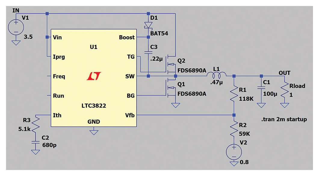
Figure 3. A simulation tool such as LTspice® from Analog Devices can be used for initial testing of the circuit. Image used courtesy of Bodo’s Power Systems
In the worst-case scenario, in which the switching regulator is not yet switched on but the auxiliary voltage has already been applied, the current IFB through the resistive divider will charge the output capacitor to voltages above the set voltage. This can happen when the load has a very high impedance. It may be necessary to install a minimum load to avoid this.
The accuracy of the auxiliary voltage at the resistive divider (1 V in Figure 2) contributes directly to the accuracy of the generated supply voltage. Thus, an especially clean voltage with low ripple should be used. Additionally, not every voltage converter is suitable for this type of operation. For example, the measuring range of the current sense amplifier in a dc-to-dc converter might only provide for an operating range at higher voltages. It should also be noted that generating very low voltages at quite high input voltages requires a low duty cycle. Here, it might be helpful to choose a switching regulator IC with a short minimum on-time and to operate it at a low switching frequency.
For operating a linear regulator or switching regulator with lower output voltages than intended by the IC manufacturer, an initial check using a simulation tool such as LTspice from Analog Devices is useful. Figure 3 shows an LTC3822 circuit with an additional voltage source as a bias for the feedback path. In this circuit, an output voltage of 200 mV is generated. According to the datasheet, the LTC3822 is suitable for generating minimum output voltages of 0.6 V. In a circuit, the auxiliary voltage, voltage source V2 in Figure 3, could be implemented with an LDO regulator or a voltage reference. With the trick described here and thorough testing of the circuit, even lower output voltages can be generated.
About the Author
Frederik Dostal studied microelectronics at the University of Erlangen in Germany. Starting work in the power management business in 2001, he has been active in various applications positions including four years in Phoenix, Arizona, where he worked on switch-mode power supplies. He joined Analog Devices in 2009 and works as a field applications engineer for power management at Analog Devices in München.

Image used courtesy of Bodo’s Power Systems
This article originally appeared in Bodo’s Power Systems magazine.