Facebook
 Google
 GitHub
 Linkedin
Dissecting the GaN ePower Stage IC-Based Inverter for Battery-Powered Motor Drive Applications
This article highlights EPC discrete eGaN FETs and Integrated Circuit ePower™ stages.
GaN transistors and ICs allow increasing power density in motor drive applications by eliminating electrolytic capacitors in the input filter. The superior switching behaviour of GaN helps to remove dead time and obtain un-matched sinusoidal voltage and current waveforms for smoother, silent operation.
Introduction
Battery-operated motor drive applications have a DC Bus voltage that spans from 24 VDC to 96 VDC. Typically, silicon MOSFETs are used in the inverter and the PWM frequency is kept below 40 kHz. The dead time in the modulation is kept in the range of 200 ns to 500 ns. In this scenario, most of the power dissipation is due to conduction losses, since PWM frequency is kept low to avoid the switching losses penalty that may become quite high with Si MOSFET.
Figure 1 shows an inverter integrated in the motor and connected to the battery with cables. During its switching operation, the inverter generates a ripple on the voltage and on the current on the battery cables that become major source of EMI. An LC filter is then inserted between inverter and battery cables to reduce the interference. As an example, the LC filter in an ebike application is made of an inductor L = 6μH and two electrolytic capacitors of C = 330 μF.

Figure 1: Cables from the battery are the source of EMI and require the insertion of an LC filter at the inverter input
EPC GaN devices show lower switching losses when compared to Si MOSFET and do not have a body diode pn junction so there is no associated reverse recovery in hard switching operation. These two factors combined help to eliminate the dead time and to increase the PWM frequency to a point that the input filter made of one inductor and one or two electrolytic capacitors can be substituted with ceramic capacitors. The advantage is quieter operation with a smaller and lighter inverter. And, last, but not least, moving from electrolytic to ceramic capacitor reduces cost and increases system reliability.
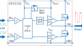
Figure 2 shows the EPC9146 inverter boards equipped with three ePower™ stage EPC2152 ICs used for the experimental tests with and without input filter reported in this article.

Figure 2: (a) EPC9146 modified with L=6μH and two C=330μF input filter (b) EPC9146 modified with two C=22μF ceramic capacitors (c) EPC9146 showing the three EPC2152 eGaN ePower™ stage ICs
Switching behaviour
Three factors contribute to the behaviour of a device during the switching event:
- Reverse capacitance CRSS
- Body diode reverse recovery
- Power loop and common source inductance due to package and layout
Reverse capacitance CRSS
When analysing the hard switching behaviour of a given device, it is essential to consider its reverse capacitance (CRSS) characteristics, its linearity, and the ratio between its low voltage value and its high voltage value (CRSSslow/CRSShigh). In fact, CRSS plays a major role during the switching event, and the observed dvDS/dt between drain and source is inversely proportional to CRSS and directly proportional to the Igate current flowing in the gate during the Miller Plateau. Ideally, a CRSS constant vs. voltage would simplify the gate driver design because the designer could just size the gate driving resistor to obtain the desired dv/dt slope. In reality, CRSS value varies with applied VDS voltage and, depending on the technology used, the non-linearity affects the overall switching event. 7
Conventional gate driving is done by applying a voltage to the gate of the switch through a resistor. If the value of the ratio CRSSlow/CRSShigh is too high, either of the following conditions can occur:
- the switch is too fast at the beginning of the turn-on event, leading to high dv/dt
- the switch is too slow at the end of the turn-on event, leading to a tail effect and higher power dissipation
In Figure 3 the curves of CRSS vs. voltage of a 100 V MOSFET and of a 100 V eGaN FET are shown. The commutation waveforms of the eGaN device are smoother because the CRSS curve is more linear than the MOSFET.

Figure 3: (a) Silicon 100 V MOS (BSC027N10NS5) has CRSSlow/CRSShigh = 1500 pF/35 pF = 4 (b) GaN: EPC 100 V eGaN® FET, an EPC2022, has CRSSlow/CRSShigh = 300 pF/6 pF = 50
Body diode reverse recovery
In a MOSFET there is an intrinsic body diode that has an important effect in the hard-commutation of a half bridge leg. When a MOSFET in a half bridge is turning on against the body diode of its complementary switch, it must deal with the reverse recovery current, that depends on load current and on the turn on di/dt [2]. In MOSFET based motor drives, it is a common habit to slow down the turn-on event to reduce di/dt and to reduce the reverse recovery current; this requires however to increase the minimum dead time that can be applied to the half bridge.

Figure 4: (a) Voltage modulation and phase current at 20 kHz with500ns dead time

Figure 4b: Voltage modulation and phase current at 20 kHz with 21ns dead time
In a GaN FET, the absence of an intrinsic body diode and its associated reverse recovery allows having a repeatable and smooth dv/dt that in turn allows reducing the dead time.
Power loop and common source inductance
The package common source inductance and the power loop inductance in the layout is responsible for the switching node ringing, which is a source of EMI noise. In conventional MOSFET inverters, designers reduce the dv/dt to reduce the ringing at the expense of a longer dead time. The common source inductance can be virtually eliminated, and the power loop inductance can be reduced to 400 pH when using a chip scale package discrete eGaN FET with optimal layout. If an eGaN integrated circuit is used, then the inductance can be further reduced. This removes the lower limit on the dead time that can be virtually eliminated in a motor drive eGaN inverter.
Dead time reduction effect – silent operation
When using discrete eGaN FETs or a GaN ePower™ stage IC in an inverter for motor drive, the dead time can be reduced to tens of nanoseconds allowing a smooth voltage waveform applied to the motor terminals. Figure 4 shows the difference in terms of modulation voltage and the phase current between two different dead time values. Eliminating the dead time improves the quality (in terms of THD) of the applied sinusoidal voltage that is in turn reflected in less distortion in the phase current and less vibrations and acoustic noise generated by the motor. A video that allows the difference to be heard can be found at the following link: https://youtu.be/nr80sdYyL-M
PWM frequency increase effect – Reduction of input filter
An eGaN inverter can be easily operated at 100 kHz PWM frequency thanks to its lower switching dissipation and smoother switching at the allowed dv/dt. Considering the worst case of a pure inductive load to simplify the equations, it can be obtained that the input voltage ripple is a function of the inverter output peak current, the input capacitance value and the PWM switching frequency [3]:
$$\Delta\upsilon _{pp} = \frac{1}{f_{sw}}\frac{I_{0}}{C_{f}}
As first order approximation, if the PWM frequency is from 20 kHz to 100 kHz, the input capacitance can be reduced by at least a factor of five to preserve the same input voltage ripple. The capacitor technology plays a role, so by increasing the PWM frequency the reduction factor is bigger than the theoretical. This will be explain in the next section.
$$\Delta I_{D} \cong \frac{\Delta V \cdot D }{f_{PWM}\cdot L}\propto \frac{1}{f_{PWM}}$$
The input current ripple is inversely proportional to PWM frequency. During a PWM cycle each half bridge leg of the inverter can be considered equivalent to a buck converter at constant current and similar formulas apply:
Capacitor technology effect on input voltage and current ripple
With low PWM frequencies (20 kHz) the required input capacitance requires the designer to use polarized capacitors; electrolytic or Tantalum. The electrolytic capacitors pose limits on the amount of the RMS current they can support, and it is common to see at least two in parallel in the input filter. Tantalum capacitors have lower capacitance density per volume then electrolytic counterparts, and they are expensive.
When the PWM frequency is increased, the minimum needed capacitance decreases allowing the use of ceramic capacitors. This brings in several advantages to the design because ceramic capacitors exhibit lower series impedance with a minimum in the region between 100 kHz and 200 kHz, are more stable in temperature, and are more reliable. The overall result is more compact and reliable inverter, given the same power dissipation and power output.
Figure 2 shows the difference in space occupation between 2 x 330 μF electrolytic and 2 x 22 μF.
Figure 5 shows the input current ripple, the input voltage ripple and the output current ripple when comparing a
- conventional inverter with LC input filter at PWM = 20 kHz DT = 500 ns L = 6 μH C = 2 x 330 μF
- eGaN inverter without input filter at PWM= 100 kHz DT = 21 ns C = 2 x 22 μF.

Figure 5: (a) Conventional inverter with LC input filter at PWM = 20 kHz DT = 500 ns L = 6 μH C = 2 x 330 μF eCaps – Phase U current 500 mA/div – Input voltage 200 mV/div – Input current 200 mA/div –50 μs/ div zoom timescale

Figure 5: (b) eGaN inverter without input filter at PWM = 100 kHz DT = 21 ns C = 2 x 22 μF ceramic – Phase U current 500 mA/div – Input voltage 200 mV/div – Input current 200 mA/div –10 μs/div zoom timescale
In Figure 5 both inverters are running an ebike motor at 36 VDC battery voltage and 5 ARMS phase current. It can easily be seen that the input voltage and current ripple are similar, so even if the second solution at 100 kHz does not have input filter, the same conducted EMI as in first solution with filter at 20 kHz is expected. In the second solution the output current ripple is reduced and the current in the motor has a better sinusoidal shape.
Effect of PWM frequency increase on the output voltage spectrum
Moving from 20 kHz to 100 kHz PWM frequency also brings other effects that needs to be taken into consideration. Figure 6 shows the spectrum envelope [3] comparison between lower frequency and slower dv/dt and higher frequency and higher dv/dt PWM. Increasing the PWM frequency shifts the spectrum content to higher frequencies, so to get the full advantage of eGaN inverter technology it helps integrating the inverter into the motor. The power cables to the motor may be sources of EMI too, but they get reduced to the minimum when an Integrated Modular Motor Drive (IMMD) approach is followed.

Figure 6: Inverter output voltage spectrum envelope – blue 20 kHz 5V/ns – red 100kHz 12V/ns
Conclusion
Many battery powered motor applications are moving from conventional Si MOSFET low PWM frequency inverters into GaN high PWM frequency inverters. The advantages rely on the elimination of the electrolytic capacitors, and the input inductor. EPC discrete eGaN FETs and Integrated Circuit ePower™ stages are then the perfect choice to take the advantage and to increase the power density to a new level.
References
[1] A.Lidow, M. De Rooij, J. Strydom, D. Reusch, J. Glaser, “GaN Transistors for Efficient Power Conversion.” Third Edition, Wiley. ISBN 978-1-119-59414-7
[2] J. Glaser, D. Reusch, “Comparison of deadtime effects on the performance of DC-DC converters with GaN FETs and silicon MOSFETs”, 2016 IEEE Energy Conversion Congress and Exposition (ECCE)
[3] M. Vujacic, M. Hammami, M. Srndovic, G. Grandi, "Analysis of dc-Link Voltage Switching Ripple in Three-Phase PWM Inverters," Energies. 2018; 11(2):471. https://doi.org/10.3390/en11020471.
This article originally appeared in Bodo’s Power Systems magazine.
About the Authors
Marco Palma holds a Bachelor's Degree in Electronics Engineering earned at Polytechnic University of Turin (Politecnico di Torino) and also has an MBA earned at SDA Bocconi. Marco worked as the Director, Systems and Applications at International Rectifier where he has the responsibility to define new smart products for appliance and light industrial market consisting in multi-die ICs in single package. His main focus is to expand the business mainly in European market and support business unit to expand further in Asia.