Facebook
 Google
 GitHub
 Linkedin
DAB Calculations for 3kW Battery Charger App & Magnetics Design
The dual active bridge topology is currently raising a lot of interest from the power electronics community. Its bidirectional nature, soft switching and high-efficiency features make the DAB a perfect candidate for high-power applications like battery energy storage systems.
Basics
In Figure 1, the basic DAB configuration is shown in the Frenetic Circuit Simulator. In simple terms, it is two full bridges with a transformer that separates them in the middle, and with symmetry being one of the characteristics of this topology. It’s easily inferred that, with proper control, power can be bidirectionally transferred from any of the bridges to the other. Notice that the transformer is modeled as an ideal transformer in parallel with a certain magnetizing inductance and a series leakage inductance. In the DAB topology, the leakage inductance is a key specification parameter.
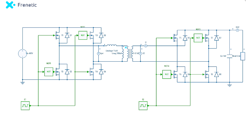
Figure 1. The basic DAB configuration. Image used courtesy of Bodo’s Power Systems [PDF]
Controlling a DAB
In Figure 1, C1 and C2 control modules drive each bridge independently, having the same frequency. C1 or C2 can introduce a phase shift between signals, controlling their respective bridge. There is also the option of a third phase shift between C1-C2. Therefore, there are three phases in total that can be controlled.
We have the Single (SPS), Dual (DPS) and Triple Phase Shift (TPS) control methods, where naming implies the number of free variables for control. The simplest case is SPS, where the phase shift between C1 and C2 is the one manipulated. SPS is easy to use and has high efficiency with ZVS, in particular at heavy load, acceptable current stress, and relatively low reactive power when the output-input voltage gain is close to one. Also, the phase shift between mosfets in each bridge is fixed at 180° for both C1 and C2. To achieve the best performance throughout the wide power and voltage range, DPS has been developed, particularly to maintain ZVS and restrict the switching current at the medium load. In DPS, the phase shift between the legs of a bridge is not necessarily fixed at 180° but is the same for both C1 and C2. In TPS, C1 can have a different phase shift than C2 and it is advantageous at light load or even no-load condition securing ZVS for all switches.
SPS Control Method
SPS is the easiest control method to implement. Of course, there are disadvantages if compared to DPS or even TPS, but efficiency and ZVS for all mosfets are not in this list. Therefore, SPS is a reasonable choice for a charger application, at least.
As mentioned above, the leakage inductance is a key spec parameter. In a DAB, the leakage inductance, which can be increased by introducing a series shim inductor, controls the limit of the maximum available power for transfer.
For SPS:
\[L_{lk}=\frac{T_{SW}(1-D)DV_{in}V_{o}n}{2P_{max}}\,\,\,\,\,(1)\]
\[D=\frac{phase\_shift}{\pi}\,\,\,\,\,(2)\]
Where D is the parameter with values 0 to +/-1 indicating a phase shift between C1-C2 from 0° up to +/-180°.
Worth mentioning that in (1) the term D (1-D) actually controls the power output, given that the other parameters like Llk, n (transformer turns ratio), Vin or Vo stay the same. This term maximizes its value at D=0.5, which translates using (2) into a 90° phase shift. More or less phase shift than 90° will result in lower output power. If the sign of D is negative, that implies a negative phase shift and means that the power travels the other way.
In theory 90°C ≤ Dπ ≤ -90°C is all it’s needed to control the maximum power output and its flow, but in reality the practice is to design for max power output at a +/- 60°-70° phase shift, limiting the reactive currents inside the bridge that would result in unnecessary losses. The higher the phase shift, the higher the reactive currents, thus the rms currents and the losses in the bridges.
\[d=\frac{nV_{o}}{V_{in}}\,\,\,\,\,(3)\]
Vo: is the output voltage
Vin: is the input voltage
n: is the transformer turns ratio (Vpr/Vsec)
ZVS Area
The SPS topology offers full zero-voltage switching for all x8 switches, when operating under certain conditions. Unfortunately, turn-off losses exist, but the mosfet driving circuitry can effectively minimize them. That said, targeting an efficiency goal of 95-97% design is within reach. That effort is however compromised if the DAB doesn’t experience ZVS. The following equations describe the necessary phase shift to achieve ZVS in the two bridges:
\[D>\frac{d-1}{2d}+\frac{2\sqrt{L_{lk}C_{eq\_i}}}{Td}\,\,\,\,\,(4)\]
\[D>\frac{1-d}{2}+\frac{2d\sqrt{L_{lk}C_{eq\_o}}}{T}\,\,\,\,\,(5)\]
LIK: transformer leakage inductance (or the sum of transformer leakage and the inductance of a series inductor to increase the total available inductance).
Ceq_i: Input bridge equivalent mosfet Coss + transformer parasitic capacitance
Ceq_o: Output bridge equivalent mosfet Coss + transformer parasitic capacitance
T: switching period
Using (4)(5), graphs similar to the one presented in Figure 2 are obtained.
Notice the “ZVS zone” in Figure 2. Equation (4) describes the “leading FB” condition to achieve ZVS and marks the upper boundaries in Figure 2, above the d=1 line. Respectively, equation (5) sets the necessary condition for the ZVS of the lagging bridge. Choosing a phase shift that satisfies both equations means that ZVS is achieved in all switches. This implies a minimum D, thus a minimum power output as described in (1).
Also, when the phase shift is low, in a light load scenario, there is a strict margin for ZVS operation. Keeping the d ratio close to 1 is the way to solve this problem and maintain ZVS. In a battery charging application, there is a mode of constant voltage until power goes down as the battery approaches its full charge drawing less and less power from the DAB. That’s a light load scenario in this application.
Table 1 is the specs table for the charger application. As mentioned, the value of d (output to input voltage ratio) should be as close as possible to 1, especially at light loads, to stay within the ZVS zones, so the turns ratio should be selected accordingly.
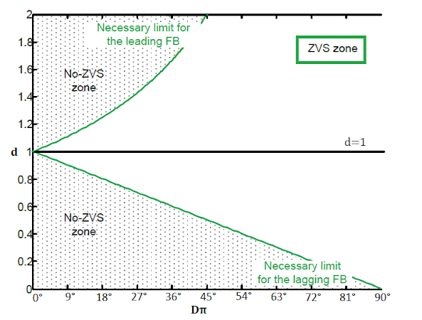
Figure 2. ZVS areas in SPS. Image used courtesy of Bodo’s Power Systems [PDF]
When the battery voltage is high (i.e., an almost charged battery pack) the turns ratio should result in a d=1 value. Solving (1) for a maximum output voltage of 54V, n=8.5. On the other hand, when the battery is discharged (47V) with a selected n=8.5, then d=1.14. For manufacturing reasons n=8 was finally selected.
The leakage inductance is given from (1), choosing a maximum phase shift at 60° or Dmax=60°/180° = 0.33, then Llk=52uH. The minimum power at which ZVS is achieved highly depends on the Coss of the mosfets in each full bridge leg. Taking a typical case of 200pF of leg capacitance on the HV bridge (primary winding) and 2000pF at the LV bridge (secondary winding) from (4)(5) to achieve ZVS in all switches the minimum power output should be between 620W and 1230W when the battery voltage moves from 47V up to 54V.
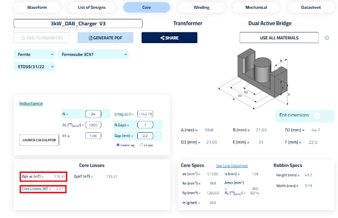
Figure 3. Transformer core selection and losses. Image used courtesy of Bodo’s Power Systems [PDF]
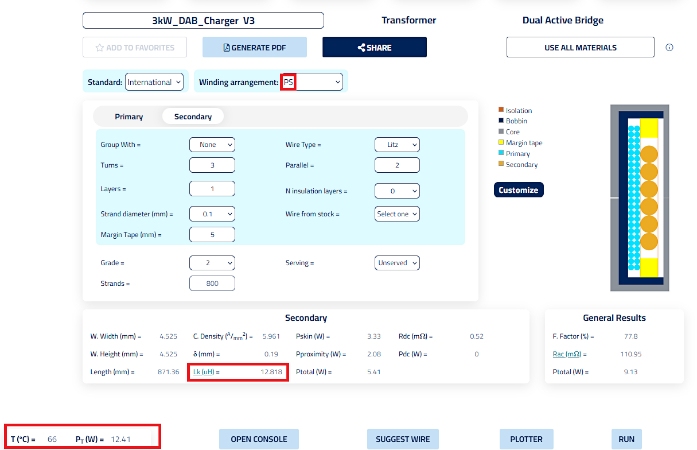
Figure 4. Transformer windings and losses. Image used courtesy of Bodo’s Power Systems [PDF]
Magnetics Design
All the necessary parameters to model and choose the transformer and/or shim inductor are now known. The parameters of Table 1 are given as input to Frenetic Online and in Figure 4 the core selection is ongoing. The important parameters of the core, marked in red, are calculated in real time as the engineer finetunes the gap of the ferrite cores, the number of turns in the primary winding etc. A ETD59/31/22, C97 material core was chosen, with a 0.2mm gap and 24 turns on the primary winding. A flux density swing at 116mT and core losses at 3.27W are acceptable.
Table 1. 3kW DAB specs
| DAB charger example | |
| Parameters | Value |
| Vin | 400V |
| Vout | 47-54V |
| Pmax | 3kW |
| fsw | 100kHz |
| n | 8 |
| Llk | 52uH |
In Figure 4, the transformer windings are chosen. The PS (P: primary, S: secondary) winding arrangement keeps the layer number down, achieving low proximity losses. Two primary windings (180strands x 0.071mm Litz wire) of 24 turns are connected in parallel at the pins and for the secondary two (800strands x 0.1mm Litz wire) wires are wounded together in a bifilar manner. Keeping the current density for the primary and secondary winding at a maximum of 5-7A/mm2 is a good rule of thumb. The AI tool has calculated a 12.8uH of leakage inductance for this transformer configuration. Given the fact that 52uH of leakage inductance is needed, a shim inductor of 39.2uH can be placed in series with the transformer. A different winding strategy like the two-chamber approach will have more leakage current for the same gapped core. However, in order to keep the total losses of the transformer low, a more conservative approach was chosen as a first iteration. Notice the yellow areas marking the position of margin tapes to keep a creepage distance at 5mm between windings. Choosing margin and insulation (between layers) tape with a CTI index >600V the design complies with IEC61558-1 standard for a reinforced isolation transformer. Finally, the total losses of the transformer at 3kW of power output are calculated at 12.4W, with a hotspot temperature of 66°C in a 25°C ambient room temperature environment.
Conclusion
In this article, the basic theory of the dual active bridge was presented, in order to design a 3kW DAB transformer used in a 48V LiFePO4 pack battery charging application. The SPS control method was analyzed focusing on identifying the ZVS operating areas of the leading and lagging bridge. The battery voltage during high and low state of charge was taken as input to properly select the transformer turns ratio. After deriving all necessary specs, Frenetic Online was used to simulate and design the transformer.
This article originally appeared in Bodo’s Power Systems [PDF] magazine.
Featured image used courtesy of Adobe Stock
Related Content