Facebook
 Google
 GitHub
 Linkedin
Biricha Lecture Notes on Analog and Digital Power Supply Design Part 2C
This article discusses how to design a compensator for all hard switched forward type peak current mode converters without optocoupler feedback.
In the previous article, we discussed how to design a compensator under-voltage mode control. In this article, we are going to look at how to compensate a peak current mode controlled Forward type converter. Peak current mode control has some advantages compared to overvoltage mode control including inherent current limiting, because if offers better line regulation and easier current sharing across multiple power stages [1].
For now, we will only look at the hard switched non-isolated converters and the design method presented here, which can be applied to all forward type converters under peak current mode control without an optocoupler. We will discuss isolation and other topologies in later articles.
Peak Current Mode Control
Before we begin our compensator design, let us first look at how peak current mode control (PCMC) works.
The operation of the converter, at first glance, is quite simple. The circuit for a PCMC Buck converter is shown in Figure 1.
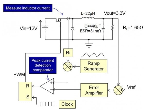
Figure 1: PCMC of a Buck Converter
As you can see, the switch in this Buck converter is being controlled by a set-reset flip-flop/latch. At the beginning of our switching period, the clock pulse sets the output of the SR latch high. This turns ON the switch at the frequency of the clock, which is, therefore, our switching frequency.
With PCMC, we typically measure the switch current. The peak of this is the same as the peak of the inductor current scaled by the current sense gain Ri. If there is a power transformer, then, of course, this will also scale the current. As you can see from Figure 1, this is fed into a peak current detection comparator. The other input to the comparator is the demand value of the peak of our current.
In other words, we are comparing the current that we want (our demand current) with the current that we are actually getting (our measured current). As soon as the actual measured current becomes equal to the current that we want, the output of the comparator circuit goes high, resets the latch and therefore turns OFF the switch. During the next cycle, our demand current may change, and that would mean that we would turn OFF the switch as soon as the actual current hits the new demand value. Thus, we are controlling the peak of our inductor current.
But, how do we set the demand value of our current? Looking at Figure 1 again, we can see that we also have a voltage loop formed by the error amplifier and its compensating components. The output of this part of our circuit creates the demand value of our current.
In short, we compare our actual output voltage with our demand output voltage and the error, or the difference, between these two (after voltage loop compensation) sets our demand value of current. Our job, therefore, is to calculate the poles and zeros and thus the component values of this compensator.
Sub-harmonic Oscillations and Slope Compensation
One final part we have not discussed in Figure 1 is the Ramp Generator block. If we set our input voltage to minimum and our load to maximum and look at the PWM on the oscilloscope and see the PWM duty cycle trace going from thick pulse to thin pulse to thick pulse repeatedly then our converter would be experiencing sub-harmonic oscillations. This is one of the headaches of current mode.
Without getting into too much detail, the problem is that in current mode, there is effectively a complex conjugate pair of poles at half the switching frequency Fs [2] and therefore at this frequency, we will have a resonant bump; this is shown by the dashed green line in Figure 3. As the duty increases so does the Q of this double pole, until at some point the gain will cross the 0 dB axis at half switching frequency thus causing sub-harmonic oscillations i.e. instability.
In order to avoid this, all we need to do is add a ramp to our measured current so that, if these oscillations were to occur, the switch would turn OFF a little bit earlier than it would otherwise (shown by dashed red area in Figure 2). This will damp any subharmonic oscillations and cause them to decay. This is the job of the ramp generator block in Figure 1. Please note that in many modern chips this ramp is added internally so you don’t have to add it yourself.
Peak Current Mode Compensator Design
For peak current mode control the error amplifier that we use is typically a Type II compensator. The circuit for the Type II compensator is given in Figure 2. The poles and zeros are set by the capacitors and resistors in the feedback network around the compensator. This compensator type along with the concept of poles and zeros has been covered in our previous articles.
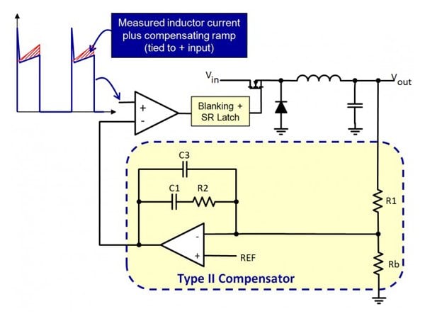
Figure 2 – Type II compensator
From the previous articles, we know the transfer function Hc(s) and equations relating the poles and zeros to component values are as follows:
`H_c(s)=(\omega_(CP0)/s)*((s/\omega_(CZ1)+1)/(s/\omega_(CP1)+1))`
Equation 1
Here wcp0 and wcp1 are the compensator’s poles and wcz1 is the compensator zero. Our job is to calculate them so that we can calculate the component values from the equations below. Please note that these poles/zeros are in radians per second but we usually work in Hz so please don’t forget to convert them if needed.
`\omega_(CP0)=1/(R_1*(C_1+C_3))`
`\omega_(CP1)=(C_1+C_3)/(R_2*C_1*C_3)`
`\omega_(CZ1)=1/(R_2*C_1)`
Biricha Digital’s automated power supply design software (Biricha WDS) automatically designs optimized compensators as discussed in the previous articles. However, if your transient response requirements are not very stringent, you can design a reasonable and stable compensator for the Forward topologies by following the steps outlined below.
Below are step-by-step guidelines on how to quickly design the compensator for this converter. All the values that we need are shown in Figure 1.
Step 1: Determine the Amount of Added Ramp Required
If your chip does not have internal ramp generation, many engineers work out the amount of ramp to add empirically i.e. set the converter to maximum duty and add enough ramps until oscillations do not occur. Alternatively, you can calculate the required amount of slope compensation (the peak-to-peak height of the compensating ramp added to the sensed current) using the following equation, which is valid for all Forward type converters and is based on [2].
VPP=(1π−0.5+D)⋅Ri⋅Ts⋅Vin⋅n2L
Equation 2
Where D is our steady-state duty cycle, Ri is our current sense gain, Ts is the switching period, Vin is our input voltage, n is our transformer turns ratio (set to 1 for Buck converters) and L is the output inductance.
This will have the effect of damping the pair of complex conjugate poles at half the switching frequency such that they have a Q of 1. As mentioned earlier, these poles are responsible for the undesirable subharmonic oscillations, which are an inherent characteristic of PCMC.
Step 2: Determine Plant Bode Plot
You don’t actually need to plot this at all but it is nice to visualize what is going on. There are many models for peak current mode converters; here we have used the popular Ridley model. For detailed mathematical analysis and equations please see [2], [3].
Figure 3 shows the Bode plot of our PCMC Buck converter. As you can see we have some low frequency/DC gain, one low-frequency real pole, an ESR zero and a pair of complex conjugate poles at half Fs. The plot will be the same overall shape for all hard switched Forward type converters. However, the plant’s low-frequency pole and ESR zero will be different but the complex conjugate pair of poles will always stay at half Fs. (Please see Article 1A for our discussion of transfer functions).
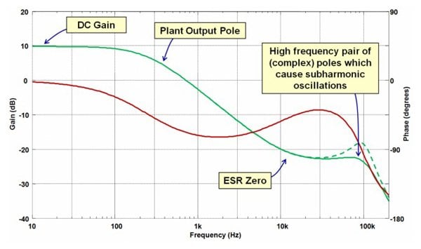
Figure 3 – Bode plot of plant stage for a PCMC Buck Converter. The green trace is the gain, red trace is the phase.
The dashed green line shows the complex conjugate poles at half the switching frequency without slope compensation. The peaking would be more pronounced with larger duty cycles. The solid trace shows what happens to these poles when we apply the slope compensation calculated in Step 1.
As you can see unlike voltage mode control discussed in the previous article, we only have a single low-frequency plant pole, followed by a zero formed by the parasitic equivalent series resistance (ESR) of our electrolytic output capacitance.
Step 3: Calculate Type II Compensator Poles/Zeros
The method presented here is an approximate method to allow you to quickly calculate the poles and zeros for a compensator with a relatively good performance for a reasonable crossover frequency (i.e. 1/10th of the switching frequency).
Our power supply design software (Biricha WDS) uses optimal algorithms, however, in this short article we will opt for this approximate method so that you can perform the calculations by hand (or perhaps with the help of your preferred math package).
You can see from the compensator’s transfer function that we have 1 pole, 1 zero and 1 pole at the origin. Please don’t forget to change to Hz (we have changed w to f in the following equations to denote this change). To get reasonable performance:
1 – Place 1 compensator pole at the ESR zero frequency to cancel the plant’s ESR zero:
`f_(CP1)=1/(2\piESRC)="11.6 kHz"`
Equation 3
2 – Place the compensator zero at 1/5th of your desired crossover frequency to give you a phase boost around crossover (remember zeros give you a phase boost – see Article 1A) Fx is the desired crossover frequency. In our case let us design for Fx
`f_(CZ1)=F_x/5="2 kHz"`
Equation 4
3 – Finally, we place the pole at origin at the frequency given in Equation 5.
`f_(cp0)=(A_1*A_2*A_3)/(2*\pi*n*L*R_L)`
Equation 5
Where A1, A2, and A3 are:
`A_1=1.23*F_x*R_i*(L+(R_L*T_S)/\pi)`
`A_2=sqrt(1-4*F_x^2*T_s^2+16*F_x^4*T_s^4)`
`A_3=sqrt(1+(4*\pi^4*C^2*F_x^2*L^2*R_L^2)/(L*\pi+R_L*T_S)^2)`
Please don’t be intimidated by these large equations - there is nothing in there that we don’t know.
Evaluating this equation for a crossover frequency of 10kHz gives us:
`f_(cp0)="25.85 kHz"`
Step 4: Calculate Compensator Component Values
Now that we know the positions of our compensator poles and zeros, we can use the equations above to calculate component values for our compensator.
As we discussed in the previous voltage mode article, you can calculate R1 and Rb based on the current that you are willing to allow through them and the reference voltage needed on the controller IC. Please refer to Article 2B for more information. By allowing 1mA of current through this pot and using the standard potential divider equations and Ohm's law we can calculate:
`R_1="750"\Omega`
`R_B="2.55 k"\Omega`
2 – Now that we know R1, by rearranging the equations for the poles and zeros above and solving for the component values we can calculate the values of C1, C3 and R2 using the equations below (please don’t forget that these equations use the poles/zeros in rad/sec so we need to convert them from Hz).
`C_1=(\omega_(CP1)-\omega_(CZ1))/(R_1*\omega_(CP0)*\omega_(CP1))`
`C_3=\omega_(CZ1)//(R_1*\omega_(CP0)*\omega_(CP1))`
`R_1=(R_1*\omega_(CP0)*\omega_(CP1))/((\omega_(CP1)-\omega_(CZ1))*\omega_(CZ1))`
Evaluating these equations gives us:
`C_1="6.8 nF"`
`C_3="1.4 nF"`
`R_2="11.7 k"\Omega`
We can easily use WDS in “manual pole/zero placement” mode to verify our calculations. WDS provides us with all the important stability parameters as well as the Bode plot. WDS Bode plot for our design is shown in Figure 4 and the stability information is shown in Figure 5.
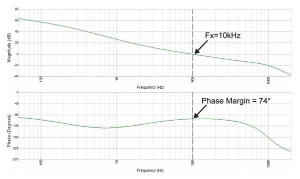
Figure 4: Simulated loop bode from Biricha WDS
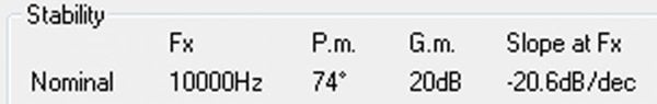
Figure 5: Stability data from WDS
From Figures 4 and 5, we can see that we have achieved a crossover frequency of 10kHz as desired and a phase margin of 74 degrees. The slope at crossover is -20db/decade and our gain margin is better than 20dB. Thus, we have designed a very stable power supply with a respectable crossover frequency and large phase margin.
Designing a Compensator
In this article, we discussed how to design a compensator for all hard switched forward type peak current mode converters (without optocoupler feedback). An approximate method has been presented that will give relatively good results in most cases.
The advantage of the method presented here is that it is quick to calculate but we do not have any control over the phase margin. Also, we included a complete numerical example down to component value selection.
About the Authors
Michael Hallworth works as a Research and Development Engineer at Birichia Digital Power since November 2012 where he is responsible for developing training material and researching new and innovative methods for the digital control of SMPS. He earned his Bachelor's Degree in Electronic Engineering and Ph.D. in Power Electronics both at the University of Reading located in England.
Ali Shirsavar holds a Doctorate of Philosophy (PhD) in Power Electronics at the University of Reading, Berkshire, England. He is an Associate Professor at the University of Reading for more than 17 years then became the Director at Biricha Digital Power.
References
- Biricha’s “Analog Power Supply Design Workshop” Manual
- Ridley, R. B., A New Continuous-Time Model for Current-Mode Control IEEE Transactions on Power Electronics, April, 1991, pp. 271- 280.
- Microcontroller Based Peak Current Mode Control, PhD Thesis, M. Hallworth
Related Content