Facebook
 Google
 GitHub
 Linkedin
Biricha Lecture Notes on Analog and Digital Power Supply Design Part 1C
This article discusses the transfer functions and role in helping engineers in designing circuits in the frequency domain, shaping the circuit's Bode plot.
In the last 2 articles we discussed frequency response analysis and loop measurement. We talked about what to look for in a Bode plot and showed what the Bode plot of a nice stable power supply should look like.
However, we still need to take the Bode plot of the plant of our power supply and with the addition of some extra circuitry change its shape so that the final Bode plot meets the stability criteria. The extra circuitry that allows us to change the shape of the Bode plot to what we desire is our compensator. Typically in analog PSUs this is just an inverting op-amp with a few capacitors and resistors. The compensator circuit is usually very simple; the hard part is calculating the correct values of the capacitors and the resistors to get the correct shape of the overall Bode Plot. How do we calculate these? Do we randomly pick a bunch of components, solder them on and hope that the power supply magically becomes stable? No, we clearly need a mathematical method of linking our capacitors and resistors to the shape of the Bode plot; this is the job of our transfer function.
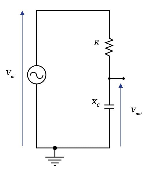
Figure 1: Simple low pass RC-filter circuit.
A transfer function is simply a mathematical model of our circuit that relates its input to its output. It follows therefore that if I have the transfer function of our system and I use a known sine wave as my input (say 1V amplitude at 10Hz), I can then calculate the amplitude and phase of the sine wave that comes out. Et voilà; we have a way of mathematically plotting the Bode plot of our system before building it.
Plotting Bode Plots from Transfer Functions
The transfer function relates the input to the output and by definition it is:
Consider the simple low pass filter shown in Figure 1. Using the potential divider equation we have:
Please note that we only use the Laplace operate “s” to simplify the algebra. There is nothing to fear about Laplace; it is just another mathematical tool to help us analyse circuits. Substituting Xc and a little bit of algebra results in my transfer function H(s):
You can see from the previous equation that the transfer function is a complex number. This is great news because it means that now as I vary the frequency f, I can plot my gain and my phase; i.e. I have a way of relating the component values R and C to the shape of the Bode plot. I have achieved my objective! Moreover, if I am not happy with the shape of the Bode plot I can influence its shape by changing the values of R and C.
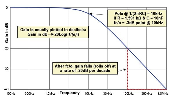
Figure 2: Gain of the low pass filter circuit, with a single pole, displayed on the Bode plot.
We know from our mathematics classes how to get the gain of a complex number:
Note that the result is not complex and therefore I can plot my gain vs. frequency which is usually done in decibels as shown in Figure 2. This is my gain plot of my Bode plot. I can now do the same thing for my phase. I know from school mathematics, how to work out the phase of the complex number. In my case this will be:
Again this equation is not complex and therefore I can plot my phase vs. frequency to get the phase plot of my Bode plot. This is shown in Figure 3.
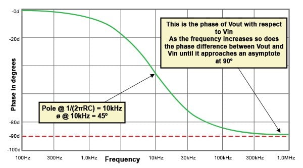
Figure 3: Phase of the low pass filter circuit, with a single pole, displayed on the Bode plot
Poles, Zeros and Their Use
The poles of a transfer function
The transfer function of our simple low pass filter takes the form of
Where in our case α= 2πRC. If we vary s from –infinity to +infinity as some point s will become equal to -1/2πRC and thus the denominator of our transfer function becomes zero. At this point the “numerical value” of my transfer function will become infinity (even though mathematicians would call this “undefined”, for us engineers infinity will suffice). Please note that this does not mean that the output voltage becomes infinity, it only means that the numerical value of the transfer function becomes infinity.
This is called the pole of my system. In other words whenever the numerical value of my transfer function goes to infinity, I have got a pole in my system. And the only the reason I am trying to determine the locations of the poles (and later the zeros) is because they tell me a lot of information about the stability of my power supply. The values of R and C are shown on the gain plot and you can see that we have a pole at 10kHz.
Characteristics of a pole in the transfer function
There are really only 2 things that you need to know about poles:
1 – Every pole in our transfer function (located in the left hand side of the s plane) will result in the gain to fall at a rate of 20dB per decade after the pole frequency. This means that after 10 kHz, every time our frequency goes up by a factor of 10, our gain falls by 20dB i.e. a factor of 10. This is clearly shown on the gain plot. If I had 2 poles in my system then the gain would fall at a rate of 40 dB per decade.
2 - Every pole in our transfer function will result in a phase lag of 90° at frequencies much higher than the pole frequency. You can clearly see from the phase plot that at high frequencies the phase approaches -90° (i.e. a phase lag of 90°). If I had 2 poles in my system then I would expect a total phase lag of 180°.
The zero of a transfer function
Sometimes our transfer function takes the following form:
We have already discussed the pole in the denominator, so let us now concentrate on the numerator. Now as we vary s from –infinity to +infinity at some point s will become equal to -1/β. This is called a “zero” of our transfer function as at this point the “numerical value” of the transfer function will become zero. Again this does not mean that the output voltage will become zero and again I am only interested in the position of zeros because they tell me information about the stability of my system.
A zero (on the left hand side of the s plane) is a little bit like an “antipole” so every time you have a zero in your system, the gain rises by 20dB per decade and you get a phase lead of 90°. If you had two zeros the gain would rise at 40dB per decade and you would get a phase lead of 180°.
aSo why am I interested in the position and the number of my poles and zeros? We can see that as the designer, I can place my pole at a certain frequency by choosing the appropriate values of R and C and therefore control the shape of the Bode plot. I can therefore start manipulating the shape of the Bode plot in order to make it fit the stability criteria.
How Well Does the Transfer Function Match with Reality
As mentioned earlier we use transfer functions in order to have a mathematical tool to design our circuits. But how well do Bode plots simulated mathematically using transfer functions match with reality? Well, there is only one way to find out; let us measure one.
Earlier in this article, we simulated a low pass filter with R =1.59kΩ and C = 10nF giving us a pole frequency of 10kHz. We can see from simulated plots earlier that at 10kHz our gain is -3dB, our phase is -45°, our high frequency phase lag is 90° and the slope after 10kHz is -20dB/decade.
We will now measure a real low pass RC filter with R = 1.6kΩ and C = 10nF using a Bode 100 network analyser from OMICRON Lab. If the hypotheses above are valid then we would expect the real measurement to be very close to the simulated one.
Figure 4 shows our real measurement. You can see clearly that we have an almost perfect match with simulations.
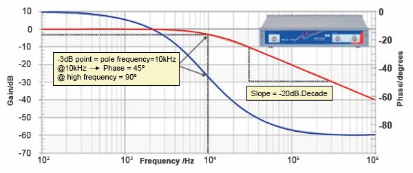
Figure 4: Real measurement of the low pass filter circuit using the Bode 100.
Concluding Remarks
In this article we discussed transfer functions and their role in helping us design circuits in frequency domain. In essence we can shape the Bode plot of a circuit by appropriate placement of its poles and zeros. Moreover, we can position the poles and zeros by appropriate selection of the circuit components such as the resistors and the capacitors.
Power supply designers use a circuit known as a “compensator” in order to force the power supply to meet the stability criteria as well as other performance targets. In analog power supplies this almost always consists of just an inverting op-amp with poles and zeros which the designer places by correct calculation of Rs and Cs.
In the previous articles we studied Bode plots and stability criteria; here we covered transfer function, poles and zeros and how to place them. We now know all the foundation material needed for stable compensator design.
In the next article we will discuss power supply compensators, their transfer functions, their poles and zeros and how to design them in frequency domain.
About the Author
Ali Shirsavar holds a Doctorate of Philosophy (PhD) in Power Electronics at the University of Reading, Berkshire, England. He is an Associate Professor at the University of Reading for more than 17 years then became the Director at Biricha Digital Power.
References
- Biricha Digital’s Analog Power Supply Design Workshop Manual
- OMICRON Lab website
Related Content