Facebook
 Google
 GitHub
 Linkedin
Making the Most of Three-Level NPC Topology
This article looks at two chipset combinations to highlight the importance of understanding how the target parameters affect the selection of chips and modules.
Three-level NPC topologies are popular choices for solar, UPS, and energy storage applications these days. The unique requirements of each application play a key role when selecting the components for a power module. A universal standard chipset is not always the best solution. This article looks at two chipset combinations to highlight the importance of understanding how the target parameters affect the selection of chips and modules.
Neutral-point-clamped (NPC) topology was introduced in the early 1980s [1], but it was not until the solar boom of the late 2000s that this topology saw wide use in power modules such as the flowSOL0-NPI family Vincotech introduced in 2008 [2]. The development of 650 V IGBT technologies contributed significantly to further extend the usage of this topology not only in solar but also in UPS and energy storage applications
Even if these applications share some similar characteristics, their requirements are not all the same. These differences have to be considered when choosing components. No universal standard solution with a single chipset can strike the right balance between cost and performance for every scenario. But chip combinations tailored for each application can better help to obtain the most competitive solution.
How NPC Topology Works
Figure 1 shows an NPC topology's switching pairs with the following components for each mode:
- Buck mode: T11-D11 ; T12-D12
- Boost mode: T13-D13 ; T14-D14
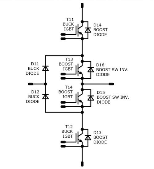
Figure 1. NPC topology with switching pairs
At full positive active power (Cos(φ)=1), commutation takes place between the buck IGBTs and diodes, while the boost IGBTS are permanently on in their corresponding half of the sinusoidal wave. There are two things to consider for this working point: For one, buck components have to be selected with the best trade-off between conduction and switching losses for the target frequency in mind. For the other, the boost IGBTs should have the lowest possible saturation voltage to minimize conduction losses.
At full negative active power (Cos(φ)=-1), the NPC operates as a power-factor corrector (PFC), in which case the boost components commute while the buck switches are off and the buck diode's losses are exclusively down to conduction. This is why the boost components play the major role in the selection process. Again, the best chip combination for the given target frequency is the set with the best trade-off between speed and conduction losses.
The switching pattern for the remaining working points at which reactive power is generated or consumed (-1<Cos(φ)<1) combines buck and boost modes. One or the other is the dominant cause of overall losses, depending on the power factor. This is why it’s important to consider the target window for reactive power capability when seeking the best components for the job.
Figure 2 outlines the switching modes for a positive half-wave:
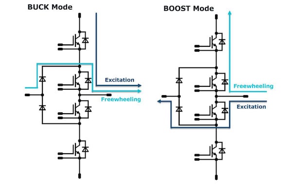
Figure 2. NPC buck and boost mode switching for the positive half-wave
Comparing and Selecting Chipsets
Various suppliers have developed new 650 V IGBT families. Very low Vce_sat IGBTs, medium speed IGBTs (up to 50 kHz approximately), and ultrafast IGBTs (up to 100 kHz) are available to target a wide range of frequencies, so there are plenty of options out there.
The frequencies of most applications that are a good fit for NPC topologies range from 16 to 32 kHz. Low Vce_sat IGBTs and medium speed IGBTs are usually the components of choice for these performance requirements.
The options are even more numerous when it comes to diodes. Anything goes from rectifier diodes with low forward voltages to ultrafast diodes with low recovery losses.
Although this article compares just two chipsets in a 100 A power module with a flow 0 housing, Vincotech offers several more combinations. This wide selection of standard modules goes to meet each customer's and application's requirements. Table 1 shows the components selected for the modules compared here:
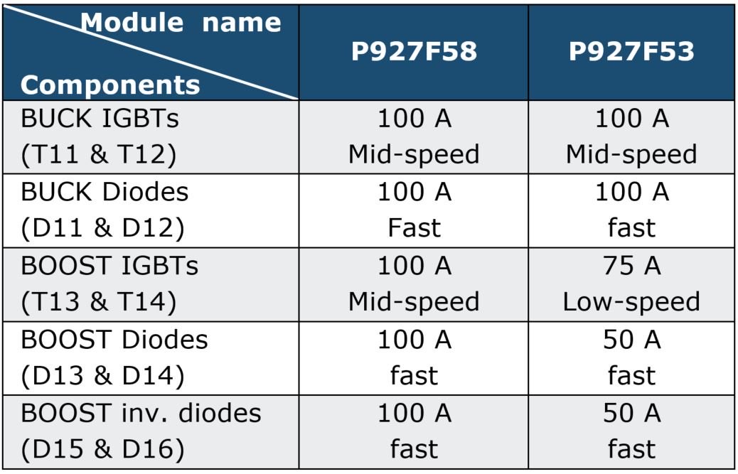
Table 1. flowNPC 0 chipsets in 100 A modules
The P927F58 module has fully rated fast components in all positions. This combination enables four quadrant operation at almost constant efficiency. Losses fluctuate from one switching pair to the other depending on the phase angle.
The P927F53 module's boost components have been modified to achieve maximum efficiency at full positive active power and to reduce costs. At this working point, the boost IGBTs are permanently on and generate conduction losses only, so that a low Vce_sat switch will achieve the best possible performance. This component provides some reactive power, but the switching losses soon dominate, which limits the range of the phase angle. The anti-parallel diodes (D13-D16) have half of the current rating at all positions to allow for some reactive power. These diodes recover fast enough to rule out very high losses and voltage spikes.
A user's module choice will depend on the application's target parameters such as switching frequency or reactive power capability. Figures 3 and 4 shows efficiency versus output phase angle for 16 kHz and 32 kHz, respectively. The P927F53's efficiency decreases significantly as the phase angle increases, while the P927F58 delivers nearly constant performance at all working points.
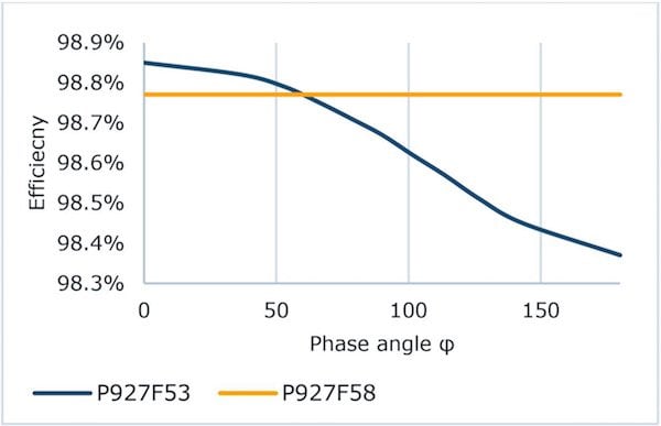
Figure 3. Efficiency vs. phase angle; conditions: 700 VDC; 16 kHz; 230 VAC; 48 A (rms)
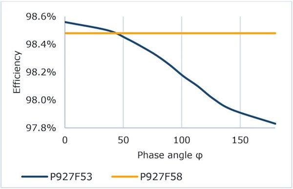
Figure 4. Efficiency vs. phase angle; conditions: 700 VDC; 32 kHz; 230 VAC; 48 A (rms)
At 16 kHz, the P927F53—that is, the module that has been optimized for active power— achieves nearly 0.1% higher efficiency at full active power. It delivers better performance until the phase angle is at 60° power (Cos(φ) = 0,5), at which point the low Vce_sat IGBTs' increased switching losses begin to dominate. At higher phase angles (lower Cos(φ)), the IGBT junction temperature rise to a level that might compromise the component’s lifetime. Moreover, the anti-parallel diodes have half of the IGBT's current rating, so they will also limit the reactive power capability.
When switching at 32 kHz, the boost IGBTs' losses dominate at a lower angle, decreasing the cross-over point between the two modules to 45° (Cos(φ)≈0,7). At full active power, the P927F53's efficiency is still better by almost 0.1%. However, the temperature difference between the IGBT junction and heat sink (ΔTj-hs) already reaches to 40°C at a phase angle of 45°. The viability of this option also depends on the selected package's or heat sink's ability to dissipate the losses.
The results vary slightly at low load and near the current's zero crossing when the IGBTs can go to zero voltage switching (ZVS) mode. At this working point, the boost IGBTs contribute with additional switching losses even at full active power. Efficiency drops further in the P927F53 module with slow boost IGBTs, shifting the cross-over point to a lower phase angle. However, this module still delivers the best performance at full active power.
Another important aspect to consider is cost. Figure 5 shows a normalized cost comparison for the two modules. The optimized module clearly has a significant cost advantage.
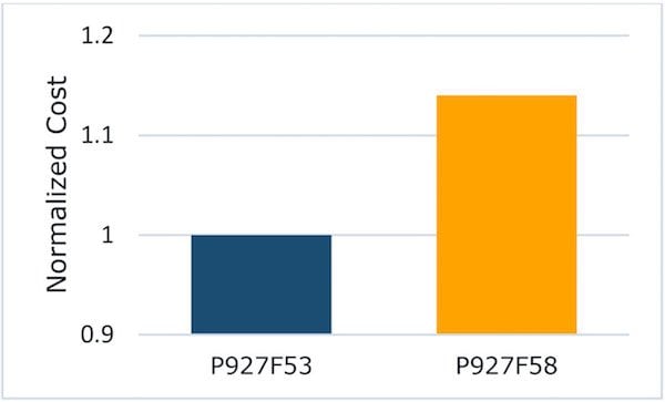
Figure 5. Normalized cost comparison for the P927F53 & P927F58
Choosing a Module
Once the performance and cost are compared, the final decision will depend on application’s requirements and the specific target parameters of each user.
The P927F58 provides a good balance between efficiency and cost for applications where the device needs to have full reactive power capability or the ability to work in all four quadrants with high efficiency. This might be the case of Energy Storage Systems or UPS with a wide reactive power range.
On the other hand, the P927F53 delivers the bigger benefits in terms of cost and performance when the primary goal is to achieve the highest efficiency at active power and the device doesn’t need full reactive power capability. This could well be the case with solar PV inverters and UPS for modern data centers.
Conclusion
The market offers a wide variety of components that can be combined in multiple ways in an NPC topology achieving different outcomes. Understanding the target requirements of each application and customer is essential to finding the most competitive solution for each case. A universal standard chipset does not always provide the most optimal result. This is why application-specific solutions and design flexibility in the power module can bring customers an added value to their final product.
About the Author
Guillem Gargallo holds an Engineers degree in Energy Management and Systems Technology at the Polytechnic University of Valencia and an MBA at Distance Learning Institute, Beuth University of Applied Sciences Berlin. He works as the Product Marketing Manager at Vincotech with a strong technical background in the implementation of semiconductor modules for industrial applications.
References
- Mikami, W., Nagataje, K. & Ono, T. (1981). A New Neutral-Point-Clamped PWM Inverter. IEEE Transaction on Industry Applications, IA-17, 518-523
- Frisch, M., Temesi, E. (2008). High Efficient Topologies for Next Generation Solar Inverter
This article originally appeared in the Bodo’s Power Systems magazine.