Facebook
 Google
 GitHub
 Linkedin
World’s First Normally-Off Gallium-Oxide MOSFET Fabricated
FLOSFIA has successfully demonstrated a gallium-oxide (α-Ga2O3) normally off MOSFET. The world-first α-Ga2O3 normally-off MOSFET comprises of N+ source/drain layer, p-type well layer, gate insulator, and electrodes. The gate threshold voltage extrapolated from I-V curve was 7.9V. The device is made of a novel p-type corundum semiconductor which functions as an inversion layer.
This is a ground-breaking work since there has been no theoretical study predicting p-type material which is compatible with n-type Ga2O3 until the FLOSFIA team discovered p-type Ir2O3 in 2016, and thus it has been considered challenging to realize normally-off MOSFET.
FLOSFIA plans to manufacture corundum α-Ga2O3 power devices, GaO™ series, starting from SBD in TO220 and then MOSFET, which will be integrated in ac adopters, driver circuit of robots, electric vehicles, home appliances, power conditioner for solar cells, and so on. The GaO™ has a potential to miniaturize inverters down to tenths of and driving cost down to half of conventional ones while maximizing conversion efficiency.
 I-V curve of normally-off Ga2O3 MOSFET.
Minimizing conversion loss of power devices is critical in order to realize energy-saving society. For power devices, silicon dominates, generating sales of more than $20 billion per annum.
However, the silicon power devices are far from perfect. When deployed in power systems, 10 percent of electrical energy can be wasted as heat − and addressing this weakness is not easy, because silicon devices are approaching their theoretical limit. Industry has been challenging to achieve higher efficiencies with new semiconductor materials.
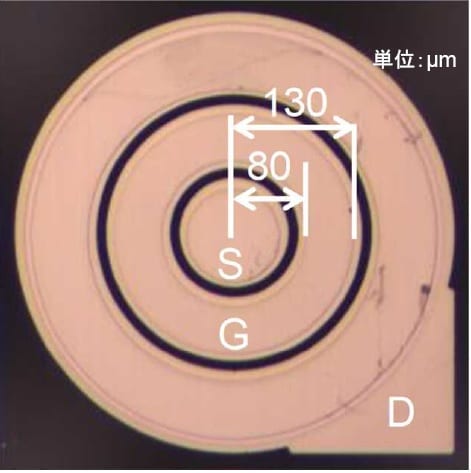 Optical micrograph of normally-off Ga2O3 MOSFET.
Gallium Oxide (Ga2O3) is a very promising material for the next generation power devices. It comes in five different phases with its α-phase which takes the corundum crystal structure possessing the most attractive material properties. Kyoto University demonstrated the world-first single crystal growth of corundum α-Ga2O3 on sapphire in 2008.
In 2015, FLOSFIA fabricated α-Ga2O3 Schotty barrier diode (SBD) showing specific on-resistance of 0.1mΩcm2, the world's lowest specific on-resistance ever. FLOSFIA, then, launched an engineering sample of α-Ga2O3 SBD packaged in TO220, a big step toward commercialization.
Another challenge FLOSFIA has been taking is to demonstrate corundum α-Ga2O3 MOSFET. In 2016, FLOSFIA and Kyoto University jointly discovered p-type Iridium oxide (Ir2O3), which has the same corundum structure as the α-Ga2O3, could be expected to form a gallium oxide-based power MOSFET.
FLOSFIA Inc., headquartered in Kyoto, Kyoto prefecture, Japan, is a spin-off from a research of Kyoto University, specializing in film-formation by mist chemical vapor deposition (CVD). Making use of physical properties of gallium oxide (Ga2O3), FLOSFIA has devoted to development of low-loss power devices.
FLOSFIA succeeded in a development of a Schottky Barrier Diode (SBD) with the lowest specific on-resistance of any SBDs currently available on the market (through an internal investigation), realizing technologies linked to power loss reduction that is reduced up to 90 percent less than before. FLOSFIA produces a variety of thin films, enhancing MISTDRY™ technology, achieving commercialization of power devices, and realizing application of its technology to electrode materials, oxide compounds with functional properties for electronic devices, plating and polymers.