Facebook
 Google
 GitHub
 Linkedin
Sumitomo Electric Launches 99% Defect Free SiC Epitaxial Wafers
Utilizing its multi-parameter and zone (MPZ™) control technology and 30-year experience in compound semiconductor development, Sumitomo Electric has succeeded in developing a high-quality SiC epitaxial wafer, "EpiEra™", and entered mass production stage.
Using MPZ™, Sumitomo Electric's SiC growth technology that adjusts various parameters depending on the area and time zone utilizing simulation and monitoring techniques. Parameters include temperature, pressure, gas reactions, and others.
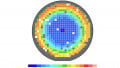
EpiEra™ has achieved an industry-leading 99% defect-free area (an area with no surface defect or basal plane dislocation (BPD) on the wafer surface), eliminating surface defects (morphological irregularities on the epitaxial layer surface that impact device yield) and Basal Plane Dislocations (dislocations generated on the basal plane in a SiC single crystal that impact the long-term device reliability) . This improves its quality, stability and reliability.
 4-inch EpiEra™ BPD map
Sumitomo Electric showcased this product at International Conference on Silicon Carbide and Related Materials (ICSCRM) 2017 held in Washington D.C., USA on September 17-22, 2017.
The Company continues to contribute to the SiC-based power electronics industry through the development of SiC devices with even higher efficiency and lower energy consumption.
SiC power devices are used in a growing range of applications such as power transmission, trains, automobiles, and electric appliances. They are increasingly required to offer higher efficiency at lower energy consumption.
SiC-based devices are expected to be a key component for energy-efficient solutions, and the demand is rapidly growing. However, to satisfy this demand and to compete with the yields and reliability of Si-based devices, material improvements are necessary.