Facebook
 Google
 GitHub
 Linkedin
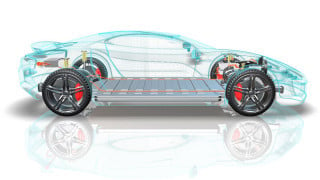
Researchers Unveil New Gallium Nitride Transistor Technology
Researchers from CNRS France and ETH Zurich have succeeded in producing high-performance high-electron-mobility transistors (HEMTs) made of gallium nitride (GaN) on a silicon(110) wafer. This makes these transistors compatible with current complementary metal oxide semi-conductor (CMOS) chips based on silicon of the same crystal orientation. CMOS chips are generally produced on silicon wafers with the so-called (100) or (110) crystal orientation. GaN, on the other hand, could previously only be used on (111)-silicon until now.
This new development makes it possible to construct hybrid electronic components that combine the computational power of the CMOS chip and the power handling capability of GaN transistors, which means power electronics can be made even more compact. Transistors are used in high-voltage circuits, for computation, and to amplify electrical radio-frequency signals. Until now they have predominantly consisted of silicon. However, electrical engineers recently began to exploit the advantages of gallium nitride for the construction of power electronics to develop faster, heat-resistant and above all energy-efficient transistors.
Gallium nitride technology was once deemed too expensive to replace silicon technology. However, researchers such as Bolognesi and his French colleagues are succeeding in growing gallium nitride on a silicon wafer, which makes the technology more economical. For the substrate, they used pure silicon with a specific crystal orientation. Known as silicon(110), the substrate costs around fifty cents per square centimeter, which is much cheaper than the usual substrates, sapphire or silicon carbide (SiC), which cost about five dollars, or even twenty dollars/cm2 in the case of SiC. Moreover, using silicon, large wafers measuring thirty centimeters in diameter can be produced, which is not possible with sapphire and SiC. However, because GaN and silicon have different material properties, it is difficult to combine the two materials on a wafer; cracks may form during heating, for instance, as the materials expand to a different degree. However, Colombo Bolognesi’s French research colleagues have now found ways to grow GaN on silicon(110) and get around the problem.
"Most transistors in the world are still based on silicon," says Bolognesi. This semiconductor does not just serve as a substrate, but also the base material of transistors and chips. "Pretty much everything in electronics is still made of silicon. It’s a fabulous material," confirms the ETH Zurich professor; "God’s gift to engineers."
However, silicon also has its drawbacks. At high temperatures above 200°C silicon-based components begin to malfunction. Gallium nitride transistors, on the other hand, can withstand temperatures of up to 1000°C, which makes the material attractive for building sensors in car engines, for example. Moreover, GaN can withstand electrical fields that are up to fifteen times stronger than in silicon; the electrons also move more quickly in GaN than in silicon, which enables faster circuitry. "This is especially important for telecommunications since the information is processed more rapidly and efficiently," said Bolognesi.