Facebook
 Google
 GitHub
 Linkedin
Researchers Discover a Method to Measure Electric Fields Inside Semiconductor Devices
Researchers at the University of Bristol discovered a method to quantify electric fields with a semiconductor device which would lead to the development of more efficient semiconductor devices.
Semiconductors, due to their electrical properties, are used for making integrated circuits and other discrete components like diodes and transistors. Semiconductor materials are useful because their electrical conductivity can be modified with dopants or external electromagnetic radiation. Designing semiconductor devices is a very complex problem and often can be trial and error. The design process is carried out commonly using accurate device models.
Device models help to analyze and predict the device behavior in a circuit design, and these models are created based on solid-state physics, such as the doping profile of the devices. The device model tries to capture the electrical behavior of that component, which then provides a basis for the manufacturing of components for real-world applications.
New semiconductor materials are emerging rapidly due to the growing demand for more compact, faster, and high-performance semiconductor devices. The accuracy of the device models is often unknown for such devices as they are only based on the IV characteristics sensed. Therefore, it is necessary to figure out how to extract relevant information from the device concurrently during operation.
Researchers at the University of Bristol have discovered a method to measure the electric field inside a semiconductor device. In their recently published study, the researchers describe how to accurately quantify these electric fields. The study can lead to the development of faster, more efficient, and more reliable semiconductor devices.
Quantifying Electric Fields Inside a Semiconductor Device
In this study, the researchers showed how electric-field-induced second harmonic generation (EFISHG) can be used to map the electric field inside the GaN-based transistors at a sub-micrometer resolution. A second-harmonic generation or frequency doubling is a process in which two photons with the same frequency are combined to form a new photon of twice the energy. The optical EFISHG signals have also been used to study complex behaviors of organic-based devices and envision carrier motion. The SHG light wavelengths used in these studies are generally above the bandgap of the material such that measurements restrict to the surface.

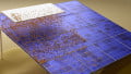
Electric field distribution in the channel of a GaN transistor. Image Courtesy of the University of Bristol
The presence of an electric field changes the intensity of the SHG light. The relationship between the applied electric field and the strength of the measured SHG light intensity provides a quantitative map of electric field distribution inside the device. The process, however, is very complex for non-centrosymmetric wide bandgap materials such as GaN as they have contributions from second and third-order nonlinear susceptibility, intrinsic and applied electric-fields-induced SHG terms.
How Does Quantifying Electric Fields Help Create More Efficient technologies?
In circuits like power converters, semiconductor devices like GaN and SiC MOSFETs are responsible for switching and converting the power. Let's say we design an AC-DC converter where semiconductor devices convert AC to a DC power supply. The conversion process results in a loss of energy in the form of heat, which can complicate the thermal management of the circuit. The more efficient the device is, the less will be the loss of energy in the form of heat.
The devices like GaN and SiC MOSFETs, moreover, work at very high frequencies and voltages. Voltage spikes and the creation of a high-intensity electric field inside can damage the device permanently. When the electric fields inside the device approach the breakdown electric field, the device no longer operates reliably and correctly. Therefore, for the reliability and longevity of the device, it is necessary to quantify electric fields inside and limit them below a critical value.
For enhancing the performance of electronic circuits, accurate device models are needed, which can be derived by understanding the electric fields inside the device. The field distribution data helps examine the impact of carbon impurities in the epitaxial buffer level of a semiconductor device. Small changes in the concentration of the dopant can significantly change the electrical properties of the device. The measurements in this study showed very different electric field distribution in devices with distinct carbon concentrations, despite them having similar device terminal characteristics. Therefore, calibration using IV characteristics sensed at the device terminals is not always potent.
This technique can help us design more efficient, more reliable, faster, and low-noise semiconductor devices for various industrial applications. According to the University of Bristol news post, "This will underpin future efficient power electronics in applications such as solar or wind turbine stations feeding into the national grid, electric cars, trains and planes. Reduced energy loss means societies do not need to produce as much energy in the first place."
About the Researchers
The following group of researchers from the University of Bristol has contributed to this project: Martin Kuball, Yuke Cao, James W Pomeroy, Michael J Uren, and Feiyuan Yang. Martin Kuball and James W Pomeroy came up with the idea of the project. Yuke Cao set up an experimental procedure, conducted the experiments, and analyzed the results. James W Pomeroy provided the necessary expertise on the technique. Feiyuan Yang conducted the simulation, and Micael Uren provided significant input on the interpretation of data. Yuke Cao wrote the manuscript with the assistance of James Pomeroy., Michael Uren., and Martin Kuball. Martin Kuball supervised the project.