Facebook
 Google
 GitHub
 Linkedin
Multi-Dimensional Circuit Carriers from Additive Manufacturing
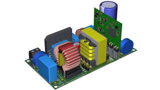
Almost all contemporary devices require a circuit board in order to incorporate one or more chips, plus the additionally required electrical components. This creates a network that fulfills a range of tasks, from supplying of electricity, circuitry, through to the output of signals.
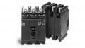
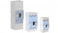
But with contemporary electronic products, the circuitry often has to compete for the limited space within the housing. When conventionally stacked, printed circuit boards (PCB) can no longer accommodate all of the necessary components, so that three-dimensional circuit carriers become the solution of choice. Here again, the ever-shorter life cycles of many devices pose additional challenges: injection molding is far too expensive to manufacture prototypes.
For this reason, The German firm of Beta LAYOUT GmbH successfully harnessed technology from EOS Electro Optical Systems (Shanghai) Co., Ltd. to manufacture and test the prototypes for three-dimensional circuit carriers: The company uses plastic parts manufactured by 3D printing. The innovation takes place after the printing process itself; once they've been made, the models are coated with a special finish that is furnished with an additive. The subsequent so-called 'laser direct structuring' (LDS) generates layouts, which can be turned into conductor tracks by activating the finish.
"We offer manufacturing of 3D-MID (mechatronic integrated devices) as prototypes for diverse companies," explains Manuel Martin, Product Manager 3D-MID at Beta LAYOUT GmbH. "Working with EOS' FORMIGA P 110, we are in a position to deliver high-quality products to our customers fast. What's particularly practical in all this is that we are even able to deal with orders of 3D models via websites and online shops. Additive manufacturing has enabled us to successfully expand our business model."
The EOS technology also provides a high degree of flexibility: the machine used is able to process various materials, including, for example, PA 3200 GF which is filled with glass beads, or the aluminum-filled polyamide Alumide. High-performance polymers such as PEEK and various metals are also available. The crucial point is that all the materials are capable of withstanding high temperatures, a limitation of the injection-molding process in series production.
Because of this flexibility, Beta LAYOUT is able to fulfill the various individual requirements of its customers, for example, by responding to the particular characteristics of the intended purpose of the circuit carrier. In this way, the company can develop individual, optimized solutions, be this in terms of lower costs, a higher degree of temperature resistance, or any other specific requirements.
Besides these advantages, additive manufacturing also offers another additional bonus: "Ultimately, what we are experiencing here is a democratization of advanced technology. Without innovations such as this, we would not be able to offer 3D-MID as a service at all," says Manuel Martin. "This would mean that many smaller companies and development houses would have no chance of realizing such prototypes.
Consequently, the much talked-about innovation and creative power of small and medium-sized companies would lose momentum and the research and development sector would be a lot less dynamic." Additive manufacturing is a catalyst for further innovation– and, in this way, perhaps a point of departure towards establishing a new Moore's Law.
Whether for individual developers or large established companies, additive manufacturing ensures that custom-made circuit carriers can be used for the prototypes of new electronic devices. The plastic components can be produced quickly and at an attractive price. The process simultaneously offers the necessary level of precision and high component-quality, allowing the required basic body to be manufactured as if it were already a close-to series product - an aspect that should not be underestimated, particularly with test runs.