Facebook
 Google
 GitHub
 Linkedin
Faster Way to 3D Print Complex & Better-Performing Electronics
UCLA engineers have developed a faster, simpler 3D-printing technique to build electronics, trimming their manufacturing time from hours down to a few minutes. The method can be used to print electronics into complex shapes in volumes that could be used for antenna arrays, prosthetics, sensors and robots. A study detailing the advance was published in Nature Electronics.
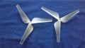
Most electronic devices today, including smart phones and laptops, use flat, two-dimensional electronics for components, such as internal sensors or antennas. Three-dimensional electronics can offer curves and shapes that help save space inside devices. And complex shapes, which can only be practically made through 3D printing, can also improve product performance, for example, by making an antenna's signal stronger.
Current 3D printing methods for electronics use multi-layer inks that are electrically conductive. This multi-step process can take several hours at a minimum and up to days in order to complete a larger build. In addition, this process can only yield simple shapes. Both are reasons why 3D electronics are not in wide use.
Recommended for you: New Technique Boosts Versatility of 3D-Printed Metals
To change that paradigm, researchers from the UCLA Samueli School of Engineering have developed a new, two-step method that cuts down the process time to only a few minutes: First, the team used a single optical 3D printer to pattern 3D shapes with pre-programmed electrostatic charges.
[video width="640" height="360" mp4=https://eepower.com/uploads/articles/Topological-Circuit-480p.mp4][/video]
Second, the researchers dipped the printed pieces into a solution that contains a dissolved material, such as electrically conducting copper. Within seconds, the material started to organize and stick itself to the designed shapes.
Not only is the new approach much faster, it also allows electronics to be built with complex shapes that have details as small as a few tenths of a millimeter.
"Our much faster and simpler method can open the door to integrating new classes of 3D electronics, such as lighter, more compact antennas for the next generation of smart phones and 5G communications, or new classes of sensors and smart materials for wearables," said, Xiaoyu "Rayne"
The new method could also be used in tactile sensors found in ultrasound machines and soft-bodied robots, said Zheng, who leads a research lab that combines additive manufacturing techniques with smart materials.
The key in instantly programming conducting materials into any predesigned 3D features is harnessing electrostatic attraction — the same phenomenon that explains why a balloon sticks to a wall after rubbing it against one's hair.
"Imagine having a blank grid with squares you can mark black, grey or white — that's sort of the same idea here as we program where electrodes go," said UCLA engineering graduate student Ryan Hensleigh, lead author of the research article. "Pixel-by-pixel, we fill a patterned grid with materials that are positively or negatively charged, or neutral.
"We then use this pattern of electric charge to deposit electrodes, conducting materials and semiconducting materials throughout the surface of a 3D-printed product," Hensleigh added.
To demonstrate their new technique's capabilities, the researchers printed several devices, including artificial fingertips that can feel the outlines of shapes and points of pressure. The lattice-like sensor has surface and internal electrodes that detect shapes when they're being squeezed.
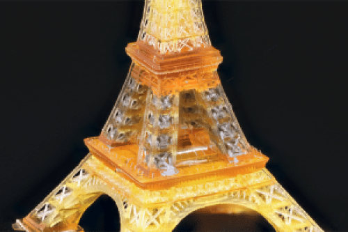
The team also built a 2-inch-tall detailed model of the Eiffel Tower, with electrodes running throughout its structure, in order to show how the method can be used to produce electronics with complex structure.
The new approach, Zheng said, can also unite multiple materials in a finished product, which the previous methods failed to accomplish. This may include magnetic materials; semiconducting materials; ceramics; piezoelectrics, which are materials that create electric charges when pushed; and carbon nanotubes, which are rolled-up sheets of carbon atoms.
Zheng started the research when he was an assistant professor of mechanical engineering at Virginia Tech. He is a member of the California NanoSystems Institute at UCLA.
UCLA graduate student Huachen Cui is the study's co-lead author. The other authors are Zhenpeng Xu and Desheng Yao, both current members of Zheng's research group; and Jeffrey Massman and John Berrigan, of the Air Force Research Laboratory at Wright-Patterson Air Force Base in Ohio.
The study was supported by the Air Force Office of Scientific Research, the National Science Foundation and the Defense Advanced Research Projects Agency (DARPA). A patent on the method has been filed.