Authors from Infineon, Fuji Electric and Vincotech Win Best Paper Honors at PCIM Asia
At this week’s PCIM Asia event in Shanghai, researchers from Infineon Technologies, Fuji Electric Co, Ltd. and Vincotech GmbH focused on various aspects of IGBTs and power modules and were awarded best paper accolades. The papers presented a range of topics including the use of IGBTs to design switching power supplies meeting "platinum" efficiency standards, the implementation of a 1-MW solar power inverter using three-level IGBT modules in parallel, and the use of parasitic inductances to reduce switching losses in power modules.
"High Speed 5 IGBT Achieves Platinum Efficiency Standard in Commercial SMPS Applications," was presented by Davide Chiola with Infineon Technologies. "Fast IGBTs have been proposed by several manufacturers as replacements for conventional or Super-junction MOSFETs due to the higher power handling capability and ultimately lower cost per Amp. However due to technological factors, there has always been only a limited utilization range where IGBTs offer both technical and commercial advantages compared to MOSFETs; for example, switching frequencies below about 100 kHz. The new High Speed 5 IGBT overcomes many of the technical limitations of previous fast IGBT generations, allowing an interesting possibilities such as ’plug and play’ replacement in several SMPS applications and topologies," stated Chiola.
The paper presented a 300W "silver box" PC power supply reference design meeting the efficiency requirements of the 80 PLUS Platinum level as set by Energy Star. The High Speed 5 technology used in this design is the high speed version of a broader technology platform called "TRENCHSTOP™ 5". It incorporates a further optimization of Infineon’s Trench Field Stop (TRENCHSTOP) concept that simultaneously reduces the switching losses as well as VCEsat. Finally, Chiola discussed the functionality of the device in different operating conditions of various hard switching and resonant topologies, highlighting advantages and limitations of an IGBT solution for SMPS.
Designing a "1-MW Solar Power Inverters using new Three-level IGBT Modules Connected in Parallel," was the topic addressed by Kansuke Fujii with Fuji Electric Co., Ltd. The topology is three-level inverter using A-NPC IGBT modules connected in parallel. According to the authors, this transformerless design represents a "first" for solar power inverters implemented with Advanced Neutral-Point-Clamped (A-NPC) topology, which utilizes Reverse-Blocking IGBT (RB-IGBT) as a bi-directional switch for clamping of its AC output to the DC neutral point.
Reaching a maximum operating efficiency of 98.5%, this 1-MW inverter consists of four inverter units in an N+1 configuration. Due to the modular structure, the new inverter offers high levels of reliability and availability. Should one of the inverter modules fail, the unit can continue to deliver its rated 1-MW output power with the three remaining units. Independent control of each of the modules is a key feature enabling this N+ redundancy. This new PV inverter is designed for outdoor operation in installations ranging up to several tens of MW, it will be commercially available in October of this year.
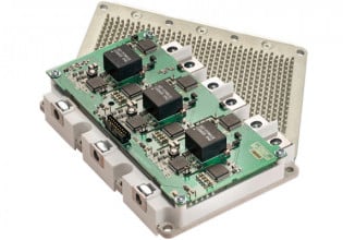
Michael Frisch with Vincotech GmbH presented a discussion of "Asymmetrical Inductance Utilized for Switching Loss Reduction In Power Modules." The new power module concept combines a low inductive turn off with the utilization of the parasitic inductance for a reduction of the turn on losses and the usage of three level switching circuits with the paralleling of fast switching components with components with low forward voltage drop.
According to the paper, increased inductance at turn on and ultra-low inductance at turn off is the new goal. This approach named "Asymmetrical Inductance" uses the parasitic inductance at turn-on and bypasses it during turn-off. A diode is used to direct the stored energy of the parasitic inductance during turn off to a capacitor. Several advantages are claimed for the new design including:
-- Superior switching performance with standard silicon switches. The new circuit improves the efficiency without investing in advanced materials such as SiC or GaN.
-- Reduced EMI: The increased turn on inductance reduces the peak current in the transistor. In other designs, this is the major source of EMI.
-- Reduced voltage swing of the onboard capacitors. The onboard capacitors will not get discharged during turn on, the voltage swing and the dissipation in the capacitors is reduced.
-- No bus bars required: Inductance in the DC-input is now welcome and will cause a further loss reduction at turn-on. In consequence the expensive laminated bus bars for a low inductive connection with the DC-capacitor bank are not required anymore. According to the authors, this might be the most significant advantage of the new approach.
More news and information regarding the latest developments in Smart Grid electronics can be found at Darnell’s SmartGridElectronics.Net.


