Facebook
 Google
 GitHub
 Linkedin
Atmel Announces High-Voltage CMOS Foundry Process with High-Density EEPROM
Atmel® Corp. announced the release of its AT35700 high-voltage process technology with double-poly, high-density EEPROM for IC foundry customers. This 0.35um technology has LDMOS transistors capable of 17V and 40V operation and has a 5.0V low-leakage CMOS core. The low-leakage CMOS has been engineered to minimize sub-threshold leakage currents making this technology ideal for portable electronic devices. Isolated NMOS and LDMOS transistors are included to minimize circuit noise. A large selection of on-chip analog resistors and capacitors are included to reduce off-chip component requirements. The technology supports placement of ESD and I/O transistors under the bond pads, thus minimizing the die size.
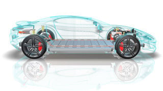
Included is Atmel's reliable double-poly, high-density memory cell. The cell can be used to create parallel, serial, or pseudo Flash memory designs. Having embedded EEPROM provides large data storage capability as required in monitor and control applications and eliminates the need for additional memory chips. This high-voltage process technology is well-suited for mixed-signal, power management, motor and motion control, and automotive monitoring and control applications. These applications can be greatly expanded with design solutions enhanced with Atmel's industry standard, workhorse AVR® microcontroller line. Atmel offers frequent multi-project wafer (MPW) runs that provide an economical means for customers to debug and prototype devices without purchasing an entire mask set. Multiple customers share the same reticle and wafer-run, thereby reducing the cost of entry.
Prices for MPW runs are dependent on the die size. Atmel also offers a wide range of mature libraries that support accurate mixed-signal simulation within the Cadence® Design Environment. The 35700 0.35um high-voltage CMOS process is available now.