Facebook
 Google
 GitHub
 Linkedin
Renesas’ New Buck-Boost DC/DC Converter Offers Ultra-Low Quiescent Current
The ISL9122A is a power-saving solution aimed at wearables, energy harvesting and battery-operated IoT devices
The new device features a forced bypass mode that presents an exceptionally low quiescent current (IQ), specced at 120nA.

Renesas’ ultra-low IQ Buck-Boost DC/DC converter. Image courtesy of Renesas
The ISL9122A also offers an automatic bypass functionality that enables the device to seamlessly transition from Boost to Buck modes when the input voltage is hovering closely to the chosen output voltage.
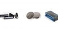
This buck-boost regulator operates from input voltages ranging from 1.8V to 5.5V, serving to extend the life of the LiB coin-cell, alkaline batteries typically used to power wearable and remote devices. The device can be controlled via an I2C input, enabling dynamic voltage scaling (DVS) in 25mV steps, with maximum output at 5.375 volts.
The unit defers to Pulse Frequency Modulation (PFM) during periods of light loads. With PFM, there are fewer “pulses” causing energy to be pressed into the output. This serves to keep the output voltage within limits, and also also improves efficiency, as fewer switches means less switching losses. Otherwise, switching frequency is 2.5 MHz.
According to Andrew Cowell, Vice President, Mobility, Infrastructure and IoT Power Business Division at Renesas, “With the explosive growth of IoT wireless connectivity applications, the ISL9122A buck-boost regulator’s fast transitions from no load to full load is ideal for powering the newest generation of devices.” He goes on to state that “Our customers praise the ISL9122A’s flexibility, dynamic voltage scaling and lowest regulated standby power consumption.”
Other Important Specifications
Low Power Requirements
- In forced bypass mode: 120 nA
- In situations other than bypass mode, IQ is still less than 1,300 nA
- Shutdown mode current is 7 nA
Forced Bypass Mode can be selected over I2C or entered automatically
Maximum Output Current is 500mA (with Vout = 3.3V and Vin = 3.6V)
Protected Against short-circuit, over-current and overheating
Minimal Requirements for External Components. Only an input capacitor, output capacitor and inductor are required

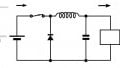
Typical application circuit for the ISL9122A. Image courtesy of ISL9122A Data Sheet
Efficiency
- Peak Efficiency: Greater than 97%
- Efficiency at 10 µA (Vin and Vout at 3.6 and 3.3. Volts, respectively): 84%
Applications
The ISL9122A and the recently released ISL9123 buck regulator are compatible with Renesas’ RL78 Family of MCUs, the RA Family of 32-bit MCUs with Arm CortexM Cores, as well as the RE Family of embedded controllers for wearables and for applications in energy harvesting.
More generally, they are also aimed at:
- Wireless earphones
- Remote IoT applications
- Water, gas and oil meters
- Portable medical devices
- Smart watches
- Wearable devices
Physical and Environmental
The ISL9122A is available in:
- An 8-bump 1.8 x 1 x 0.5 mm WLCSP package
- An 8-lead 3 x 2 x 0.9 DFN package
The device operates over an ambient temperature range of -40 to +85℃
The units are RoHS compliant
Getting to Market Faster
The ISL9122AIRN-EVZ evaluation board allows designers to more quickly evaluate the features and performance of the ISL9122A

The ISL9122AIRN-EVZ Evaluation Board. Image courtesy of Renesas
There are separate versions of the Application Board for the WLCSP and DFN versions of the ISL9122A.