Facebook
 Google
 GitHub
 Linkedin
Navitas Semiconductor Debuts 650V GaN Power IC With a 70mΩ RDS(ON)
Navitas describes the new device as the first to integrate logic, drive, protection and power all in GaN and within a single unit.
The NV6182, the latest of the company’s GaNFast power ICs, is built with an integrated cooling pad, suiting it for high-efficiency, high-density power applications
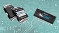
_Fig1.jpg)
The NV6128. Image courtesy of Navitas
The NV6128 is spec'd at 650 volts for continuous operation and is capable of sustaining 800 volt transients. The GaN gate is fully protected, and the device as a whole is rated to an electrostatic discharge (ESD) specification of 2,000 volts.
Member of an Established Family of Devices
The new device is the latest entry to a seven member family of GanFast power ICs. As per Gene Sheridan, Navitas CEO and co-founder, GaNFast power ICs are already widely applied to fast-charging mobile adapters of up to 200W. He states that “With the higher-power NV6128, we extended the effective power range to 500W for the consumer market and look beyond that to multi-kW data center, eMobility and new energy applications.”
Device Specifics
- VDS up to 650 volts
- VCC from 10 to 30 Volts
Drain Current
-
Continuous: 20 amps with case current at 100℃
- Pulsed for 10 µs : 40 amps and 25 amps with junction temperatures of 25℃ and 125℃, respectively
- Slew rate (dv/dt) on drain to source is 200 volts/nanosecond
- The switching Frequency is 2 MHz (max)
Thermal Resistance
- Junction to case and junction to ambient is 1.2 and 40ºC/W, respectively
_Fig2.jpg)
Simplified schematic of the NV6128. Image courtesy of Navitas’ datasheet.
The cooling pad (CP) is referenced by no less than 11 separate device pins. CP must not be left floating, and must be connected either to the power FET’s source pin or to PGND. These pins provide a thermal pathway that will allow the heat generated by the power FET to be drawn away from the device to be dissipated by the PCB
Minimized Package Inductance
Good design practice calls for minimizing the high-frequency switching noise that can be caused by parasitic inductances inevitably induced by PCB layout. To help designers to achieve this Navitas has equipped the NV6128 with two source kelvin (SK) ground pins. These pins are separate from the high current source connections pins.
Design considerations for utilizing this capability are detailed in the data sheet. This will make it possible to minimize any possible high frequency voltage spikes that might otherwise occur at the PWM input during switching.
Applications
Topologies
- AC-DC, DC-DC, DC-AC
- Buck, boost, half bridge, full bridge
- Quasi-resonant flyback
- Active clamp flyback, LLC resonant, Class D
Device Types
-
SMPS for server, telecom and networking applications
- LED lighting, solar micro-inverters
- eMobility chargers for devices such as eBikes and eScooters
- Game consoles
- All-in-one PCs
- TVs and monitors
- Gaming laptops
- Chargers and adaptors
Physical Facts
- The unit is available in a 6 x 8 mm, low inductance SMT QFN package
- The device operates over a junction temperature range of -55 to +150℃
Safety and Regulatory Concerns
ESD ratings
- HBM Human body model at 2,000 volts maximum
- CDM: Charged device model at 1,000 volts maximum
Environmental Considerations
- RoHS compatible
- REACH compliant