Facebook
 Google
 GitHub
 Linkedin
Microchip Debuts a GaN-based Ka-band MMIC for SatCom Terminals
The new monolithic microwave integrated Circuit (MMIC) delivers 10W of saturated RF output power over a 27.5 to 31GHz range
Microchip’s GMICP2731-10 allows Earth stations to transmit at high RF levels while maintaining the integrity of complex satcom modulations

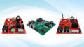
The GMICP2731-10. Image courtesy of Microchip
The GMICP2731-10 is fabricated using GaN-on-SiC technology. With a power input (Pin) of 24 dBm, the unit features a power-added efficiency (PAE) of 22% and saturated output power (Psat) of 39.5 dBm. Small signal gain at 28 GHz is 22db. Input and output return losses are both -15dB.
The unit’s balanced architecture allows it to match 50-ohm loads. It features internal DC blocking capacitors at the output, allowing for simplified design integration.
The Promise of GaN for Satellite Systems
As noted by Leon Gross, vice president of Microchip’s Discrete Products Group business unit, “As communication systems employ complex modulation schemes such as 128-QAM and as the power of solid-state power amplifiers (SSPAs) trends ever upwards, RF power amplifier designers have the difficult challenge of finding higher power solutions while at the same time reducing weight and power consumption.” He goes on to state that, “GaN MMICs used in high power SSPAs can achieve greater than 30% lower power and weight as compared to their GaAs counterparts, which is a huge gain for satellite OEMS. This product delivers on the promise of GaN and enables the size, weight, power and cost OEMs are searching for.”
Gallium Nitride (GaN) Fabricated on Silicon Carbide (SiC) Substrates
GaN substrates are still quite expensive and difficult to work with. The designer is left with two substrate choices – silicon or silicon carbide. Si is far less expensive than SiC, and it would seem the obvious choice, but there are issues.
For one, the lattices between the GaN and Si are mismatched, while GaN and SiC, on the other hand, are lattice-matched. This makes for good bonding between GaN and SiC, with the result of fewer defects and less of a problem with warping
Additionally, their thermal expansion coefficients are different, so when a GaN device grown on top of a silicon substrate is subjected to heat, the two substances will expand at different rates, threatening the device’s integrity.
Finally, GaN on SiC has far greater thermal conductivity than does GaN on silicon. This will allow the designer to tolerate more power dissipation, knowing that the heat generated can more easily be channeled away to where it can do less harm.
Electrical Characteristics
Recommended drain voltage ranges from 20 to 24 volts. The preferred gate voltage range is from –2 to –1.5V. The quiescent drain current is from 100 to 224mA.

Functional block diagram of the GMICP2731-10. Image courtesy of Microchip’s datasheet.
The maximum input power that can be tolerated is +25dBm, and the maximum gate current is 6mA. The absolute maximums drain voltage and drain current are 32V and 3 amps, respectively. For gate voltage, the maximum range is from -5V to 0V.
Applications
- 5G
- Satellite communications
- Aerospace and defense
Physical Considerations
- The unit is available in a 3.025 × 3.405 × 0.10 mm package
- Ambient temperature range is from -40 to +85 °C
Environmental Notes
The new unit is:
- RoHS compliant
- Lead-free