 Facebook
 Google
 GitHub
 Linkedin
Intel Looks to Improve Backside Power Delivery with new RibbonFET and PowerVia Architectures
Intel announced the company's future process and packaging technology roadmaps at its "Accelerated" webcast last week.
PowerVia is an industry-first for backside power delivery, while RibbonFET is Intel’s first new transistor architecture.
Improving Backside Power Delivery
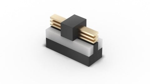
PowerVia is Intel’s take on backside power delivery, designed by the manufacturer to optimize signal transmission by scrapping the need for power routing on the front side of the wafer.
The industry-first solution features optimized signal routing to reduce power leakage and utilizes NANO through-silicon via (TSV) packaging technology 500 times smaller than most competitors, to deliver substantially increased computing performance.

The new PowerVia technology. Image used courtesy of Intel.
As explained in an article on All About Circuits, backside power delivery works considerably better than conventional methods when scaling, offering a 1% voltage margin compared to the industry-standard 10%.
This technique could therefore aid Intel to scale its solutions faster, particularly since it has also been shown to significantly decrease resistance in power delivery networks.
A New Transistor Architecture
RibbonFET is Intel’s new design of a gate-all-around transistor and represents the firm’s first novel transistor architecture since its FinFET.
The technology is designed to deliver faster transistor switching speeds while retaining the same drive current as multiple fins in a smaller footprint. In addition, also with RibbonFET Intel will offer backside power delivery.
For context, current nodes utilize FinFET transistors, but the technology is quickly being replaced by RibbonFETs.
Intel’s new RibbonFET technology. Image used courtesy of Intel.
Intel's node Intel 20A will reportedly be the first one equipped with the new transistor architecture, dubbed the '2nm' process. These transistors are reportedly smaller and faster to switch, which should also lead to better performance.
Nodes up to 3nm, on the other hand, will continue to use FinFET transistors, Intel said last year.
Moving forward, the firm said RibbonFET and PowerVia will be combined. Through the novel technologies, Intel hopes to eliminate the need for power routing on the front side of the wafer.
The goal can be reportedly achieved thanks to the fact that, in these devices, the bottom layer can be used for the power supply, while the top layer for the transistors.
This, in turn, allows wafers to be designed both more efficiently and more cost-effectively.
Intel plans to use RibbonFET in its Intel 20A process by the end of 2024.
Intel’s Accelerated Webcast
During the online event, which took place on July 26, Intel CEO Pat Gelsinger, together with Dr. Ann B. Kelleher, Intel Senior Vice President of Technology Development presented a range of breakthrough technologies.

Pat Gelsinger, speaking at the Intel Accelerated event. Image used courtesy of Intel.
As mentioned above, the webcast explored Intel’s new RibbonFET and PowerVia technologies, as well as Intel’s planned adoption of next-generation extreme ultraviolet lithography (EUV).
Often referred to as High Numerical Aperture EUV, the technology will enable Intel to receive the industry’s first High NA EUV production tool.
According to the event page on the firm’s website, the new technologies will accelerate the path back to process performance leadership as well as bolstering the company’s packaging capabilities.
What do you think about Intel Accelerated and the company’s new power technologies? Let us know in the comments down below.


Thanks for the article, Alessandro. One thing you wrote REALLY stuck out to me: “Through the novel technologies, Intel hopes to eliminate the need for external power supplies.” That is a HUGE and (IMHO) far-overreaching and generalized statement to the point of being highly misleading to your readers.
While I am just starting to dig into this new announcement, I am guessing you extracted your statement from something like this that came directly from the Intel press release: “PowerVia is Intel’s unique industry-first implementation of backside power delivery, optimizing signal transmission by eliminating the need for power routing on the front side of the wafer.” (https://www.intel.com/content/www/us/en/newsroom/news/intel-accelerates-process-packaging-innovations.html)
Eliminating some power routing at the wafer level (or even board level) is a FAR CRY from either eliminating power SUPPLIES (not mere routing) and certainly does not eliminate the need for external power supplies! I am sure I do not need to explain to you or the readers that these transistors (and any other for that matter) require power of some sort/source to run.
FYI - this is coming from a guy that focuses most of his efforts these days on Energy Harvesting so I am all about self-powered systems from ambient energies, but that is not what this is. 😉
Feel free to reach out to discuss further if you need some clarification/help from the power delivery perspective. .(JavaScript must be enabled to view this email address) http://www.linkedin.com/in/zahnstecher
Thanks again and have a great weekend!
Regards,
Brian