Facebook
 Google
 GitHub
 Linkedin
Infineon and Panasonic to Collaborate on 650V Power GaN Development
The two companies agree to joint development of the next generation of their successful Gallium Nitride (GaN) technology.
Infineon Technologies and Panasonic Corporation have just inked an agreement to extend their partnership and to commit to jointly develop and production of the second generation (Gen2) of their proven gallium nitride (GaN) technology.
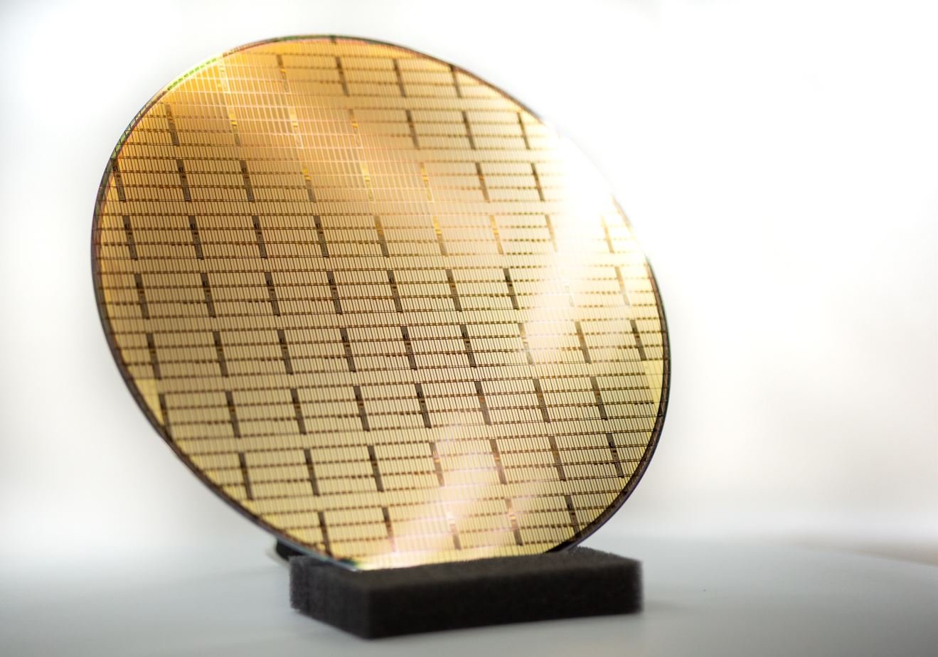
8-inch GaN on Silicon Wafer. Image courtesy of Infineon
As illustrated above, the newly developed 8-inch GaN-on-Si wafer marks Infineon’s strategic commitment to GaN power transistors, with higher sized wafers being the key lower overall production costs. In adherence to market demands, the early focus of Gen 2 will be 650 V GaN high electron mobility transistors (HEMT).
GaN vs Silicon Carbide Semiconductors
The frequency and power capabilities of GaN, silicon carbide (SiC), silicon MOSFETs, and insulated gate bipolar transistors are mapped out in the illustration below.
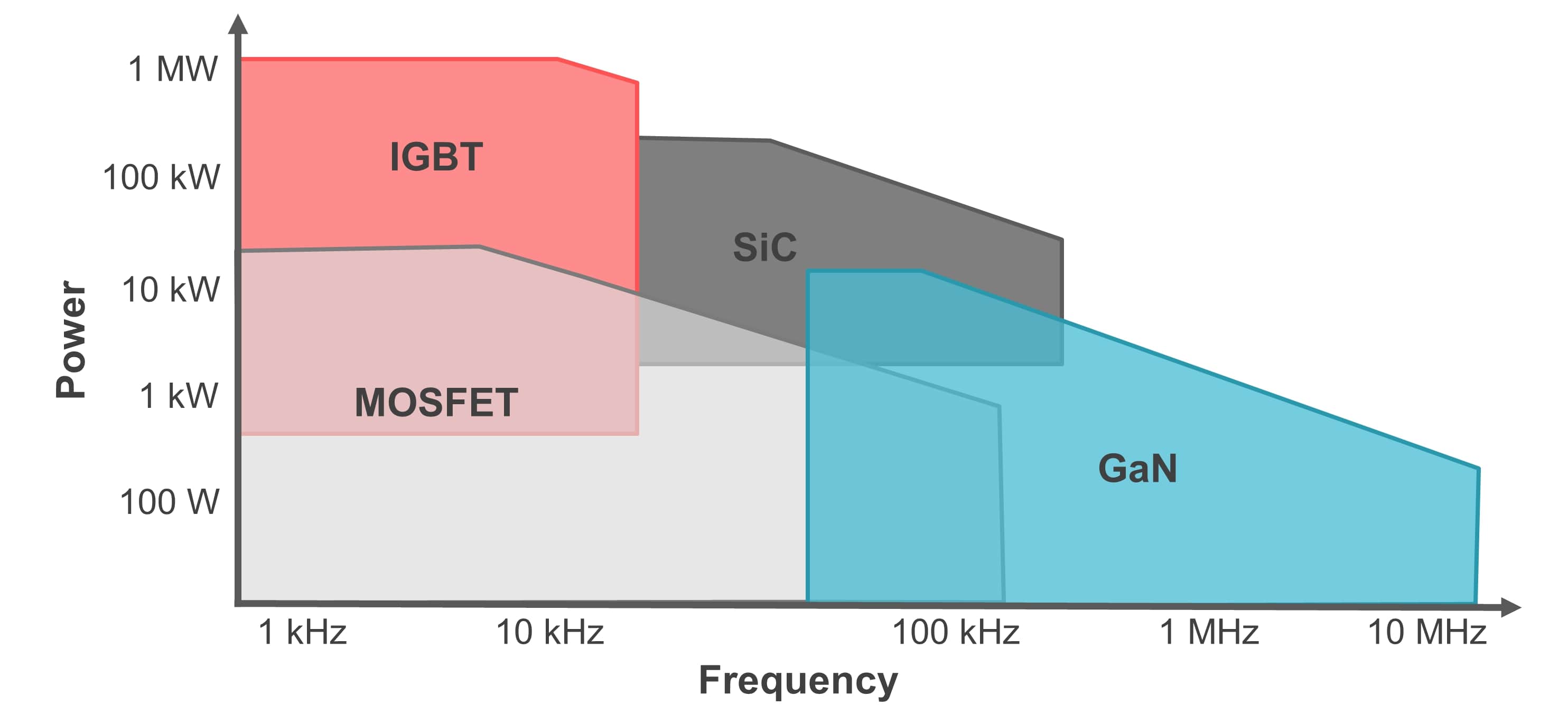
Frequency and power trade-offs between power transistor types. Image courtesy of Texas Instruments
As can be seen, while GaN devices handle somewhat less power, they can operate at much higher speed than any of the other types. For power conversion, operation at higher speeds means smaller valued, smaller sized filtering components, a vital factor in many applications where size and weight count.
They also have very low “on” voltages, meaning that when they conduct, very little energy is lost to internal semiconductor resistance. That translates into greater efficiency and less parasitic heat to deal with, both vital design considerations.
It’s little wonder that GaN devices can often be a great choice for engineers. They will be even more so as Gen 2 begins to provide increased performance specifications and, along with the larger wafer size, lower costs per part.
Previous Collaboration Between the Partners
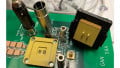
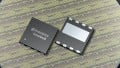
The alliance between the two companies has previously yielded the partnership’s Gen 1 power devices. These are:
What the Partners are Saying
As per Andreas Urschitz, President of Infineon’s Power and Sensor Systems Division “In addition to the same high reliability standards as for Gen 1, with the next generation customers will benefit from even easier control of the transistor as well as a significantly improved cost position, thanks to moving to an 8-inch wafer manufacturing.”
It was also mentioned in the announcement that,” Like the jointly developed Gen 1 devices, known as Infineon’s CoolGaN™ and Panasonic’s X-GaN™, the second generation will be based on the normally-off GaN-on-silicon transistor structure. This, in combination with the unmatched robustness of the hybrid-drain-embedded gate injection transistor (HD-GIT) structure, makes these components the product of choice and one of the most long-term reliable solutions in the market.”
As stated by Tetsuzo Ueda, Associate Director of Engineering Division, Industrial Solutions Company, Panasonic Corporation, “We are delighted to extend our partnership and collaboration with Infineon on GaN components. Within the joint approach, we will be able to apply Gen1 and Gen2 devices on high quality and based on latest innovation developments.”
Applications
- Switched-mode power supplies (SMPS)
- Renewable energy applications
- EV motor drives