Facebook
 Google
 GitHub
 Linkedin
IGSS GaN and SilTerra Demonstrate Powerful New Technology to Unlock US12 Billion Semiconductor Opportunity
IGSS GaN (IGaN) and SilTerra Malaysia Sdn. Bhd. are pleased to announce the impressive results of their recent technology transfer partnership, successfully demonstrating a breakdown voltage of 650V for a D-Mode MISHEMT device using 200mm GaN-on-Si wafer on CMOS compatible fabrication process.
IGSS GaN (IGaN), a Singapore-based specialist in GaN-on-silicon technology, and SilTerra Malaysia Sdn. Bhd., a home-grown Malaysian semiconductor wafer foundry, are pleased to announce the impressive results of their recent technology transfer partnership, successfully demonstrating a breakdown voltage of 650V for a D-Mode MISHEMT device using 200mm GaN-on-Si wafer on CMOS compatible fabrication process. The outcome of this exclusive collaboration results in the transfer and establishment of a gold-free metallization and CMOS compatible 200mm GaN-on-Si Metal-Insulator-Semiconductor High Electron Mobility Transistor (MISHEMT) fabrication process in SilTerra.

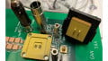
Image courtesy of IGSS GaN.
"IGaN aims to offer an innovative one-stop solution, providing 100mm to 200mm GaN-on-Si epiwafer and 200mm CMOS friendly GaN fabrication processes. This will enable customers in the power semiconductor community currently offering silicon-based power
metal–oxide–semiconductor field-effect transistor (MOSFET) and IGBTs to leapfrog into GaN technology devices, unlocking access to the huge opportunity of the US$12 billion power device market using GaN technology," said Raj Kumar, Chairman & CEO of IGaN.
“We are already engaged in positive discussions with other customers enthusiastic about the potential of our platform, keen to accelerate their access into the rapidly growing GaN market, as our new partnership with SilTerra enables mass production of this powerful new technology in early 2019,” he added.
“We are excited about this achievement to demonstrate D-MISHEMT using a 200mm GaN-on-Si wafer on foundry CMOS process. With our close partnership with IGaN, SilTerra is committed to deliver the best yielding process and capacity assurance to fulfil our mutual customers’ business expectations,” said Firdaus Abdullah, CEO of SilTerra.
GaN devices are used for high power density, wireless power transfer, allowing for higher server power, a capability recently demonstrated with great success at the APEC 2018 conference and exhibition in San Antonio, Texas. Using GaN technology, a density on-board charger (OBC) for electric vehicles delivered a three-fold increase in power density at 4kW per litre, compared to a silicon-based charger at 1.3 kW per litre. Further demonstrations revealed that GaN transistors can enable wireless charging to be increased from 100W to 1.5kW.
This innovative technology unlocks the potential for exciting wireless charging applications far beyond low power applications such as cell phones and laptops. GaN also enables greater energy savings and increased power density in data centres, which significantly reduces OPEX, CAPEX and TCO expenses, with a fifty percent power density increase achievable utilizing the same size power supply.
IGaN and SilTerra are together offering an accelerator to spur the conversion of pure silicon and compound-based technologies into GaN-on-Si. This will favourably impact the bottom line and long-term business competitiveness of both power and RF semiconductor
companies who adopt this technology. The powerful efficiency performance figures of GaN-on-Si show its further potential as a green-enabling technology, delivering a positive global environmental impact by minimizing power conversion losses.
For more information on our pioneering semiconductor and fabrication processes and partnerships, please contact us at [email protected].
About IGSS GaN
Founded in 2014 by Industry Leaders & Technologists in Singapore, IGSS GaN produces world-class GaN-on-Si Epitaxial wafers & provides wafer fab process to accelerate its mass adoption globally. We possess in-depth semiconductor technical and foundry process know-how in semiconductor and GaN-on-Si technology. The combination of best technology and process know-how have enabled us to deliver superior solutions that ensure long-term customer satisfaction. We secured state-of-the-art technologies and patents through an exclusive partnership with leading R&D institutions which lead us to develop more advanced product and solutions on GaN-on-Si targeting at power electronics to wireless communication markets. We have secured a strategic exclusive partnership with renowned foundries to provide a one-stop turnkey solution for semiconductor OEMs.