Facebook
 Google
 GitHub
 Linkedin
Bringing Micro LEDs to the Dimensions of the Silicon Industry with ALLOS’ 200mm and 300mm GaN-on-Si Epiwafers
ALLOS applied its unique strain-engineering to show outstanding uniformity and reproducibility for 200 mm GaN-on-Si epiwafers.
To address the wafer size mismatch and to tackle the yield challenge in micro-LED production, ALLOS has applied its unique strain-engineering to show outstanding uniformity and reproducibility for 200 mm GaN-on-Si epiwafers. Additionally, the company reports about its success on the roadmap to 300 mm.
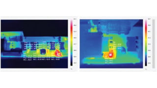
Yield plays a crucial role to make micro-LED displays successful. It has a direct impact on the manufacturing complexity and cost. To enable the needed cost reductions, large wafer diameters are essential. This is particularly true for micro-LED applications in which wafers from CMOS-lines are integrated with LED epiwafers, e.g. by bonding. Here the matching wafer diameter even has an enabling role comparing to the smaller diameters available from GaN-on-sapphire. The ALLOS team has already used its unique strain-engineering technology to push the wavelength uniformity further and further, showing 200 mm GaN-on-Si LED epiwafers on Veeco’s Propel with STDEV of as little as 0.6 nm in February 2019.
With its latest results, ALLOS can now show excellent reproducibility for this technology with a wavelength uniformity of consistently below 1 nm STDEV for 200 mm. “At the same time, we achieve all other production requirements like the bow of < 40 µm and SEMI-standard thickness of 725 µm. These parameters are very important when bonding CMOS wafers to LED epiwafers,” is added by Alexander Loesing, one of the co-founders of ALLOS, who continues, “These results are particularly impressive because our technical team is really pushing the boundaries of GaN technology only with very limited time and resources available for this work.”
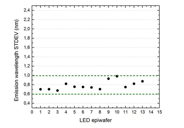
Figure 1: Reproducibility of wavelength uniformity on 200 mm GaN-on-Si epiwafers for micro LED application.
Commenting on the achievement, Dr. Atsushi Nishikawa, the CTO of ALLOS pointed out: “Already our predecessor company AZZURRO had been first in the market with commercial 150 mm and later 200 mm GaN-on-Si epiwafer products. Making 300 mm was the next natural challenge. When the first reactor designed for such large wafers, the Veeco ImPulse, became available we proceeded to tackle the challenge.”
ALLOS confirmed that its technologies scale successfully to 300 mm on this new reactor. In particular, ALLOS’ unique technologies for strain-engineering and superior crystal quality work on 300 mm as expected.
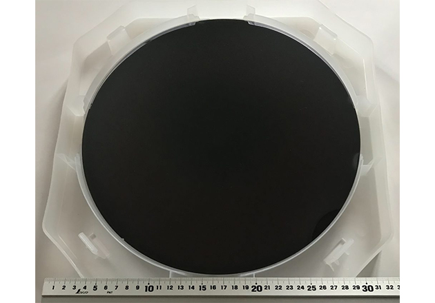
Figure 2: 300 mm GaN-on-Si epiwafer for micro LED.
“Being among the first to push III/nitride technology to 300 mm is very exciting for us. It proves how robust our strain-engineering technologies are and we are looking forward to establish this technology for micro-LED customers” is added by Nishikawa, who is also one of the co-founders of ALLOS.
Scaling up from 100 mm diameter – the typical wafer dimension for GaN-on-sapphire – has an even bigger business impact for micro LEDs than in other parts of the LED industry. Besides the well-known effects of lower cost per area when using larger diameters, the jump to 200 mm and 300 mm GaN-on-Si for micro-LED production, enables the usage of CMOS facilities that have a much lower cost and additionally higher production accuracy than conventional LED lines. A further effect arises because most micro-LED manufacturing concepts either include mass transfer technologies that are using large area transfer-stamps or monolithically integrated displays:
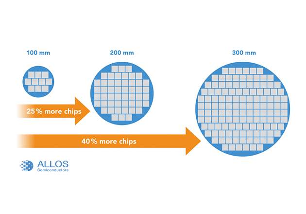
Figure 3: Scaling wafer dimensions: Additional cost-benefit by better area utilization due to matching rectangular shape of display or transfer stamp to circular shape of wafer.
Summarizing the 300 mm advantages, Loesing concludes: “For micro-LED displays, the better area utilization of larger wafer sizes can easily account for 40 % cost advantage from 300 mm epiwafers for this step alone. Together with the other cost advantages and the production benefits offered by CMOS lines, this results in leading industry players evaluating micro-LED displays based on 300 mm GaN-on-Si.”
Read and download the original version of this press release in English or Chinese (simplified).
About ALLOS Semiconductors
ALLOS is an IP licensing and technology engineering company which is helping clients from the semiconductor industry worldwide to master GaN-on-Si technology and unleash its benefits. ALLOS is providing licenses to its technology know-how and patents as well as transferring the technology to its customers’ MOCVD reactors. In addition, ALLOS is delivering customer-specific solutions as well as consulting services for next generation GaN-on-Si development challenges.