Facebook
 Google
 GitHub
 Linkedin
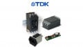
Analog Devices Digital Isolator Packaging Meets Safety Requirements in Medical & Industrial Applications
Analog Devices, Inc. (ADI) has introduced what it says is the first packaging technology for digital isolators that achieves a minimum of 8mm creepage distance required by global industry standards to ensure safe operation in high-voltage medical and industrial applications. Incorporating Analog Devices’ iCoupler® digital isolation technology, the CSA International- (Canadian Standards Association) certified package achieves 8.3mm creepage and is designed for use in advanced medical diagnostic, measurement and monitoring, and industrial and instrumentation systems that operate up to 220-250Vac. The new packaging enables designers to replace lower performing optocouplers with ADI’s digital isolators, while meeting the minimum creepage requirements necessary for these applications.
Creepage is the shortest distance over an insulating surface, such as an IC package, over which an arc may travel between two galvanically isolated conductors. To ensure adequate insulation, a 125V working voltage requires 6mm of creepage, while a 220-250V working voltage requires a package with a minimum of 8mm. The JEDEC standard 16 lead SOIC has 7.6mm of creepage measured around the end of the package and does not meet the 220-250Vac requirements to ensure safe operation in high-voltage medical and industrial applications. By increasing the length of the standard JEDEC package by 2.5mm, ADI is able to enlarge the creepage path to 8.3mm. The resulting package remains compatible with JEDEC standard footprint with minimal impact on board space.
"Analog Devices is the only semiconductor manufacturer to offer digital isolators in packaging that exceeds minimum insulation requirements for sensitive, high-voltage applications," said Patrick O’Doherty, Vice President, Healthcare Group, Analog Devices. "The new SOIC packaging makes it possible for designers of 220-250V medical equipment, such as patient monitoring devices, to migrate their design requirements from optocouplers to ADI’s extensive digital isolator portfolio. Using a single iCoupler digital isolator can reduce overall board space while delivering four times the data rate and using 90 percent less power."
ADI’s proven iCoupler technology is based on chip-scale transformers, rather than on the LEDs and photodiodes found in optocouplers. Transformers support higher data rates, consume less power, and are more stable over life compared to LEDs and photodiodes. By fabricating the transformers directly on-chip using wafer-level processing, iCoupler channels can be integrated with each other and other semiconductor functions at low cost. iCoupler transformers are planar structures formed from CMOS and gold metal layers.
A high-breakdown thick polyimide layer underneath the gold layer insulates the top transformer coil from the bottom coil, resulting in the most reliable and highest level of digital isolation available. CMOS circuits connected to the top coil and bottom coil provide the interface between each transformer and its external signals. With more than a half a billion channels deployed, ADI’s iCoupler digital isolation technology has been designed into hundreds of applications, such as USB isolation in patient monitors, where it allows hospitals and physicians to adopt the latest advances in computer technology to supervise patient health and wirelessly transmit medical records without compromising patient safety.
More news and information regarding the latest developments in Smart Grid electronics can be found at Darnell’s SmartGridElectronics.Net.