Facebook
 Google
 GitHub
 Linkedin
Advanced Packaging Innovations Improve Power MOSFET Performance
FETs from Infineon, Transphorm, and ROHM feature innovative packaging that increases performance and efficiency.
When it comes to FETs, what’s on the outside counts. The right packaging can increase efficiency, help with thermal management, and make FETs more compact. Three major manufacturers have implemented innovative packaging to get the job done.

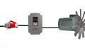
Forklift, light electric vehicle application. Image used courtesy of Infineon
The OptiMOS power MOSFET by Infineon uses a source-down package configuration for improved efficiency and performance. The OptiMOS series of power MOSFETs are low and medium-voltage (25-150 V) devices that employ an innovative source-down package design where the active side of the device (source and gate nodes) connects directly to the lead frame at the bottom of a PQFN (Power Quad Flat No-lead) package. These MOSFETs will now be carried by Rutronix, a leading electronics components distributor based in Isnpringen, Germany.
Source-down packaging allows for improved efficiency, better thermal dissipation capabilities, and easier parallelization of multiple devices in higher-power applications. OptiMOS devices are ideal for medium-voltage motor drive applications in light electric vehicles, power tools, robotics, and similar applications.
ROHM Semiconductor is also introducing five new devices that integrate two 100 V MOSFETs into a single package, as part of their HP8KEx/HT8KEx (n-channel plus n-channel) and HP8Mex (n-channel + p-channel) dual MOSFET series. The solutions are designed for improved performance and reduced size in fan motor drives used in communication base stations and industrial equipment.
Finally, Transphorm is releasing the SuperGaN TOLT FET, the industry’s first surface-mount gallium nitride (GaN) device in a JEDEC-standard (MO-332) TOLT (TO-Leaded topside-side cooling) package. The new GaN device packaging is useful for applications where conventional bottom-side cooling might not be practicable.
Source-Down Packaging
With standard drain-down packaging, the drain side of the MOSFET die is connected directly to the lead frame of the PQFN package. A copper clip is then used to create an electrical connection between the lead frame at the bottom of the package and the source node at the top of the die.

Source-down MOSFET packaging. Image used courtesy of element14
Source-down technology flips the orientation of the die, allowing the source potential of the die to be connected to the package lead frame and aligned with the thermal pad. The drain connection is then made via a copper clip.
With source-down packaging, two different footprints are available with varying gate pad locations. A center-gate footprint places the gate pad near the center of the package, while a corner-gate layout adheres to the gate location convention of the standard drain-down packaging. The latter configuration allows source-down packaged devices to be pin-compatible with drain-down devices.
Advantages of Source-Down Packaged MOSFETs
There are several design and performance advantages associated with source-down packaged MOSFETs:
- Efficiency. Source-down construction removes packaging limitations that allow for a larger die. A larger die translates to a reduction in on-resistance of up to 30%, reducing I2R conduction losses.
- Parallel operation. With the source and gate nodes of the die both facing the lead frame, it is now possible to reposition the gate connection toward the center of the package (center-gate footprint). For applications that require higher power levels, a center-gate footprint makes it much easier to operate multiple MOSFETs in parallel with the same gate drive circuitry.

Standard-Gate and Center-Gate PQFN footprints. Image used courtesy of element14
- Thermal performance. With the source connected directly to the lead frame, the thermal pad is now at circuit ground, which facilitates the removal of heat using thermal vias under the device.
These design and performance characteristics make source-down packaged MOSFETs ideal for medium voltage motor drives, switch mode power supplies, and telecom infrastructure applications.
SuperGaN TOLT FET
Transphorm’s TP65H070G4RS is a 650 V, normally-off GaN FET that consists of a high-voltage GaN HEMT and low-voltage silicon MOSFET in cascode configuration. The FET has a low on-resistance of just 72 mΩ for reduced conduction losses.
In addition to a high operating efficiency, the new TOLT device assists with thermal management by offering topside cooling from its 10 mm x 15 mm package. The SuperGaN TOLT FET follows the recent release of three surface-mount TOLL (TO-Leadless) packaged FETs and offers thermal management capabilities comparable to through-hole packaged devices while supporting high-volume manufacturing processes.

SuperGaN FET in surface mount TOLT package. Image used courtesy of Transphorm
According to Philip Zuk, SVP of Business Development and Marketing at Transphorm, the TOLT packaged devices will be targeted for high-performance computing, renewables, and electric vehicle applications.
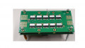
Dual MOSFET Chips for Motor Drives
The HP8KEx/HT8KEx and HP8Mex series form ROHM combine either two n-channel or one n-channel and one p-channel MOSFET devices into a single package. The MOSFETs are rated to a withstand voltage of 100 V and are designed to save space and simplify the design of fan motor drives used in base station communications and industrial equipment.
.jpg)
Backside cooling reduces dual MOSFET RDS(ON). Image used courtesy of ROHM
According to ROHM, replacing two single-chip TO-252 MOSFETs with one HSOP8 dual-packaged device can reduce the board space footprint by up to 77%. Packaging with backside heat dissipation capabilities allows on-resistances (RDS(ON)) to be reduced by up to 56% compared to other standard dual MOSFET solutions.