Facebook
 Google
 GitHub
 Linkedin
Thermomechanical Wear-Out in GaN Devices: A Focus on CSP and PQFN Packaging
GaN power devices offer high efficiency, but reliability is now a package-level challenge. CTE mismatch causes solder-joint cracking, which EPC mitigates using predictive modeling and design.
Gallium nitride (GaN) power devices are driving a new era of power conversion systems with high efficiency and high-power density for automotive, industrial, robotics, renewable energy, and data center applications.
Their enhanced switching speed and lower conduction losses compared to conventional silicon MOSFETs enable designers to greatly reduce passive components and increase overall system efficiency. But as power density continues to rise, reliability is increasingly moving away from the semiconductor itself and toward package-level interactions.
Among these package-level challenges, thermomechanical wear-out has emerged as a key reliability consideration. EPC evaluates reliability using a test-to-fail reliability methodology, where degradation mechanisms are intentionally accelerated under controlled conditions to identify the dominant wear out mechanism and develop predictive lifetime models. This approach provides a more fundamental understanding of long-term reliability than traditional pass/fail qualification tests.
The Physics Behind Thermomechanical Wear-Out
Thermomechanical wear-out in GaN power devices is fundamentally a package-level reliability phenomenon driven by difference in the coefficients of thermal expansion (CTE) among the semiconductor die, solder interconnects, copper structures, and PCB laminate. Unlike intrinsic semiconductor degradation mechanisms, thermomechanical failure develops progressively through the accumulation of cyclic mechanical strain.
EPC reliability investigations consistently identify solder-joint cracking as the dominant thermomechanical wear-out mechanism under both temperature cycling (TC) and power cycling (PC) conditions. During low-temperature operation, the PCB contracts more than the GaN die because of its higher CTE.
At higher temperatures, the opposite occurs, with the PCB expanding more than the device. Because these materials are mechanically connected through solder joints, the resulting CTE mismatch generates cyclic strain within the solder. Repeated thermal changes gradually accumulate irreversible deformation, eventually leading to solder fatigue, crack initiation and propagation.
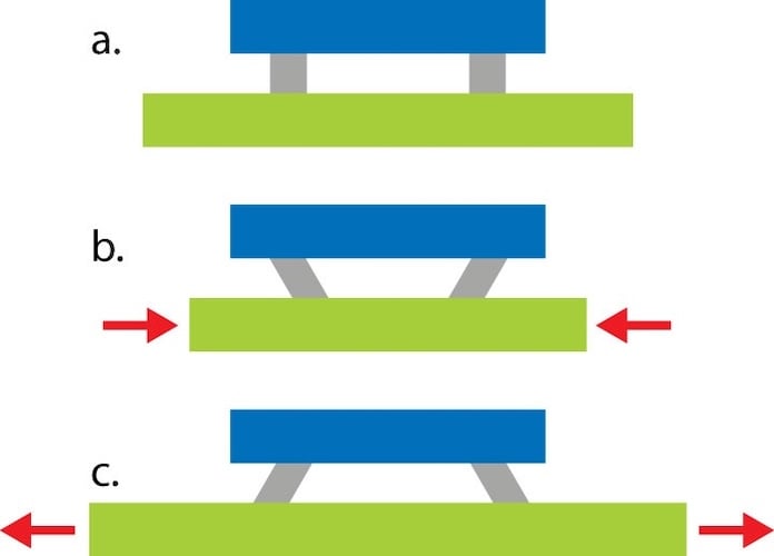
Figure 1. CTE mismatch between the GaN die, solder interconnects, and PCB generates cyclic mechanical stress during temperature excursions, eventually leading to solder fatigue and crack formation.
To model thermomechanical lifetime, EPC applies the classic Coffin–Manson fatigue framework, widely used in solder fatigue reliability studies:
$$N_f = C(\Delta \epsilon)^{-n}$$
where Nf represents cycles to failure, Δε is the cyclic strain amplitude induced during temperature excursions, and n is a material-dependent fatigue exponent. In practical terms, this relationship highlights a critical reliability reality: even relatively small increases in thermally induced strain can significantly reduce package lifetime because degradation follows a power-law behavior rather than a linear trend. EPC applies this framework as the foundation for modeling solder fatigue in wafer-level chip-scale packages subjected to thermal cycling stress.
However, the thermomechanical wearout is influenced not only by package geometry, but also by the temperature cycling conditions themselves. Experimental studies show that larger temperature swings (ΔT) increase solder fatigue and higher maximum temperatures (Tmax) increase creep-related deformation in SAC305 solder joints.
Ramp rate and dwell time also affect lifetime.by changing both the magnitude and duration of mechanical loading. To account for these variables, EPC applies the Norris-Landzberg framework, incorporating the temperature range, cycling frequency and thermally activated creep effects:
$$N_{TC} = A \cdot f^{- \alpha} \cdot (\Delta T)^{- \beta} \cdot \exp(\frac{E_a}{k T_{max}})$$
where NTC represents the expected temperature cycling lifetime, f is cycling frequency, ΔT is the thermal excursion, and the Arrhenius exponential term captures thermally activated creep processes at elevated temperature. Experimental results show increasing temperature range, ramp rate or while longer dwell time at high temperature accelerates solder fatigue and measurably reduces thermomechanical lifetime.
Thermomechanical Wear-Out in CSP Packages
Wafer-Level Chip-Scale Packages (WLCSP) are popular in GaN power electronics since they can reduce parasitic inductance and allow very compact converter designs. However, without a traditional leadframe, the solder joints directly absorb the thermomechanical stresses during thermal excursions. As a result, solder-joint fatigue becomes a key factor governing long-term reliability under temperature cycling conditions.
EPC evaluated several WLCSP GaN products, including EPC2206, EPC2071, EPC2069, EPC2218, EPC2204, EPC2152 and EPC2215, under identical temperature cycling conditions from −40°C to 125°C using SAC305 solder and two-layer PCBs. Weibull analysis revealed significant differences in lifetime among devices despite identical assembly and test conditions. Failure analysis consistently identified corner solder-joint as the dominant wear-out mechanism.
Initial analysis indicated that die size alone shows a relatively weak correlation with temperature cycling lifetime. To better understand the die geometry effect, EPC introduced the concept of Maximum Distance from Neutral Point (DNPmax). During thermal loading, the package center experiences minimal displacement, while the solder joints at the package corners are subjected to the highest mechanical strain. Consequently, solder fatigue cracks preferentially initiate at corner solder joints. DNPmax helps capture this preferential behavior and provides a physically meaningful parameter for lifetime prediction.
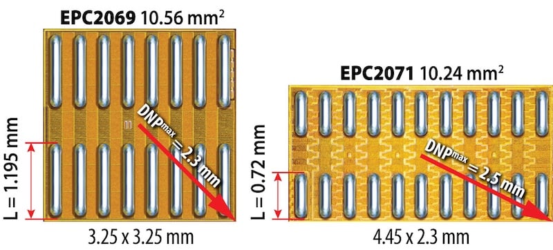
Figure 2. Maximum Distance from Neutral Point (DNPmax) defines the solder-joint regions experiencing the highest thermomechanical strain during temperature cycling.
Further analysis revealed that solder bump geometry also strongly affects thermomechanical reliability. Since corner gate bumps are the primary failure locations, EPC introduced an effective DNP parameter (DNPeff) that incorporates both device dimensions and gate bump length. By accounting for both die geometry and geometry of the critical solder joints, DNPeff provides a significantly improved correlation with measured lifetime data.
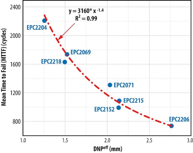
Figure 3. Measured MTTF strongly correlates with effective DNP (DNPeff), demonstrating the combined influence of die size and gate bump geometry on thermomechanical lifetime.
The resulting lifetime relationship was found to follow:
$$\text{MMTF} \propto (\text{DNP}_{eff})^{-1.4}$$
with an excellent correlation coefficient of R² = 0.99. This demonstrates that both die geometry and solder bump geometry must be considered when predicting thermomechanical lifetime.
To further validate the model, EPC performed finite element analysis (FEA) using the Anand viscoplasticity model for SAC305 solder in COMSOL. The simulations captured the thermomechanical behavior of the SAC305 solder joints during temperature cycling and showed good agreement with the experimental results. Predicted MTTF values based on Darveaux’s energy-based fatigue model were within ±10% of the measured data, providing additional confidence to the predictive thermomechanical framework.
Ramp Rate and PCB Effects
Thermomechanical reliability is influenced not only by package design, but also by the thermal profile and PCB construction. EPC observed an approximately 13% decrease in MTTF with an increase in ramp rate from 4°C/min to 14°C/min. COMSOL simulations showed that increased ramp rates generate larger stress-strain hysteresis loops within the SAC305 solder, resulting in higher energy dissipation density and enhances the rate of fatigue accumulation.
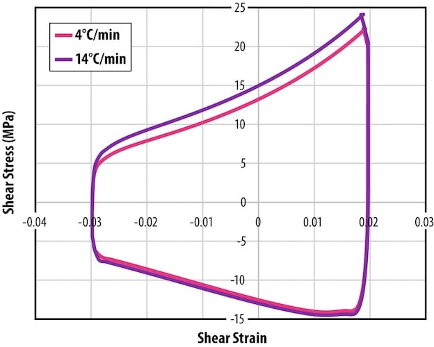
Figure 4. Solder joint stress-strain hysteresis increases with higher thermal ramp rates, thus accelerating fatigue damage accumulation.
The architecture of the PCB also plays an important role in thermomechanical reliability. High density power systems often utilize multilayer PCBs with increased stiffness. EPC observed an approximately 40% reduction in lifetime when employing a sixteen-layer PCB instead of a two-layer PCB. Thicker and stiffer PCBs deform less during thermal excursions and therefore transfer higher mechanical stresses into the solder joints.
Underfill Optimization
When projected lifetime falls below application requirements, underfill materials can dramatically improve reliability by redistributing stress away from solder joints.
EPC recommends underfills with:
- CTE values between 16 and 32 ppm/°C
- Glass transition temperatures above maximum operating temperature
- Young’s modulus in the range of 6–13 GPa
Finite element simulations revealed that excessive stiffness may reduce solder stress but transfer damaging stress into the die edge. Experimental TC testing on EPC2218A devices has shown a significant improvement in reliability with Henkel’s Loctite Eccobond-UF 1173 underfill material. Devices without underfill failed more than 50% at around 1600 cycles, while underfilled devices showed no significant degradation after 3000 cycles.
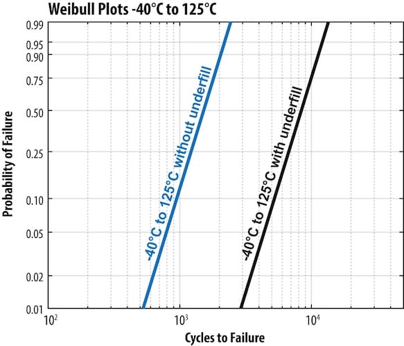
Figure 5. Proper underfill materials significantly improve CSP thermomechanical reliability by reducing solder fatigue during temperature cycling.
Thermomechanical Wear-Out in PQFN Packages
Power quad flat no-lead (PQFN) packaging is widely used for GaN power devices due to its compact dimensions, excellent thermal performance and low electrical parasitics. While the package structure differs from wafer-level chip-scale packages (WLCSPs), thermomechanical reliability remains a key design consideration. In this section, EPC examines temperature cycling and power cycling behavior in PQFN GaN devices and demonstrates that solder fatigue remains the dominant thermomechanical wear-out mechanism.
Temperature Cycling and Thermal Shock
EPC evaluated the thermomechanical reliability in PQFN packages using the EPC2367, a 100 V device mounted on a sixteen-layer PCB representative of modern intermediate bus converter (IBC) architectures. The devices were subjected to temperature cycling from −40°C to 125°C under JEDEC JESD22-A104 conditions. Electrical characterization showed that there was no variation of the threshold voltage (VTH) and RDS(on) after 1600 cycles. The cross-sectional SEM analysis showed partial cracking at the corner gate solder joint, with crack propagation limited to approximately 10% of the solder-joint length.
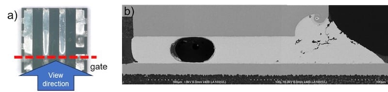
Figure 6. Optical image of EPC2367 showing the cross-section location and viewing direction. The cut was performed through the gate, the location where failure is most likely to occur. (b) High magnification SEM imaging at the gate solder joint shows no through-crack.
Thermal shock testing further demonstrated the robustness of the PQFN package. EPC2367 devices were subjected to thermal shock cycling from -55C to 150C with aggressive ramp rates of 50C/min. The electrical parameters were stable and no through-cracks were observed even after 1000 cycles. The crack propagation was limited to approximately 15% of the solder-joint length, indicating high resistance to extreme thermomechanical stress.
Power Cycling Reliability in PQFN GaN Devices
To relate the temperature cycling behavior with actual operating conditions, EPC extended the study to power cycling with EPC2302 flip-chip PQFN GaN devices.
Power cycling induces the thermomechanical stress by repeated self-heating during the device operation, as opposed to the environmental temperature cycling. EPC developed an IOL based closed loop power cycling system with the ability to precisely control junction temperature and dwell time. The devices were stressed with different power-on times (ton = 30, 50, 90, and 120 seconds) and with the same temperature limits of 40°C to 150°C.
The results demonstrated a strong dependence of the lifetime on the power-on duration. Shorter power-on times (ton) resulted in significantly longer characteristic lifetime, while extended high-temperature dwell times accelerated wear-out. The Weibull analysis showed that the dominant failure mechanism remains unchanged for all test conditions.
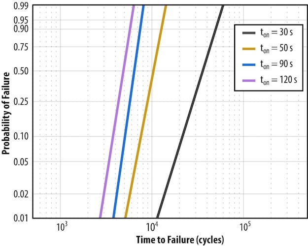
Figure 7. Power cycling lifetime strongly depends on power-on duration (ton), with longer high-temperature dwell times accelerating solder fatigue.
Failure analysis again identified corner gate solder-joint cracking as the dominant degradation mechanism. No evidence of intrinsic GaN semiconductor degradation or metallization failure was observed. The similarity between the temperature cycling and power cycling failure signatures confirmed that both stresses are governed by the same solder fatigue mechanism.
Using a modified Norris–Landzberg framework, EPC demonstrated strong agreement between COMSOL simulation and experimental results:
$$N = (3.75 × 10^5) \cdot (t_{on})^{-2.09}$$
The negative exponent indicates that increasing power-on time leads to faster creep-related deformation and fatigue accumulation within solder joints. Additional thermal measurements indicated that the reduction in lifetime was primarily due to increased lengths of high temperature dwell rather than increased thermal gradients. Further COMSOL FEA analysis verified that the corner gate solder bump was consistently the most failure-prone region during power cycling stress.
Finally, EPC’s thermomechanical reliability studies indicate that solder fatigue, not intrinsic GaN degradation, is often the dominant wear-out mechanism in advanced GaN power systems. With the continued increase in power density and switching frequency, the optimization of package geometry, PCB construction, thermal cycling conditions and underfill materials will become increasingly important to ensure long term field reliability.
Reference
GaN Reliability and Lifetime Projections: Phase 18 – EPC Report, Siddhesh Gajare, Ph.D., Duanhui Li, Ph.D., Ricardo Garcia, Angel Espinoza, Peter Tieu, Ph.D., Jordan Green, Justin Yee, David Wu, Christopher Wong, Shengke Zhang, Ph.D.
All images used courtesy of EPC.