Facebook
 Google
 GitHub
 Linkedin
Radiation Resilient and Robust: GaN Tech Propels Next-Gen Power Electronics to New Frontiers
This article examines the reasons GaN power devices work for power conversion applications in space and how their resistance to radiation makes them a robust solution for space missions.
This article is published by EEPower as part of an exclusive digital content partnership with Bodo’s Power Systems.
Space exploration has always demanded cutting-edge technology, reliability, and resilience. The latest breakthrough in power electronics, gallium nitride (GaN) technology, has emerged as a game-changer for space-based systems, offering superior radiation tolerance and unmatched electrical performance compared to traditional silicon MOSFETs.

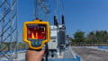
Image used courtesy of Adobe Stock
GaN’s Radiation Resilience
Space is a harsh environment in which semiconductors can experience various forms of radiation, including gamma radiation, neutron radiation, and heavy ion bombardment. GaN devices have showcased exceptional radiation tolerance, setting them apart from the silicon MOSFETs traditionally used.
An energetic particle can cause damage to a semiconductor in three ways: causing traps in non-conducting layers, causing physical damage to the crystal (displacement), and generating a cloud of electron-hole pairs that cause the device to conduct momentarily and possibly burn out in the process. In enhancement-mode GaN (eGaN) devices, energetic particles cannot generate momentary short-circuit conditions because mobile hole-electron pairs cannot be generated.

Figure 1. Cross section of a typical enhancement mode GaN (eGaN®) device. Image used courtesy of Bodo’s Power Systems [PDF]
Gamma Radiation
GaN’s unique construction and intrinsic material properties make it highly resistant to gamma radiation. eGaN devices are built very differently from silicon MOSFETs. The gate, source, and drain terminals are on the top surface. Figure 1 shows that the gate is separated from the underlying channel by an aluminum gallium nitride layer. This layer does not accumulate charge when subjected to gamma radiation. This ensures that GaN devices maintain their performance even in the presence of high-energy photons.
Neutron Radiation
Neutron radiation primarily causes displacement damage to semiconductor devices, affecting parameters like RDS(on). GaN devices exhibit minimal degradation even at high neutron exposure levels (up to 4x10^15 fluence) due to their significantly higher displacement threshold energy than silicon, as seen in Figure 2.
Heavy Ion Bombardment
Heavy ion radiation can lead to single-event effects like single-event gate rupture and single-event burnout in silicon MOSFETs. Single-event gate rupture is caused by the energetic atom causing such a high transient electric field across the gate oxide that the gate oxide ruptures. Single-event burnout is caused when the energetic particle transverses the drift region of the device where there are relatively high electric fields. The energetic particle loses its energy while generating many hole electron pairs. These hole electron pairs crossing the drift region cause the device to short-circuit between the drain and source temporarily. This short circuit can either destroy the device, called a single event burnout, or the device can survive, appearing as a momentary short circuit that can cause damage to other components in the system. The absence of a gate oxide in GaN devices makes them immune to gate rupture. Moreover, as confirmed through extensive testing, heavy ion bombardment only slightly increases the drain-source leakage current in GaN devices, well below the defect limit.
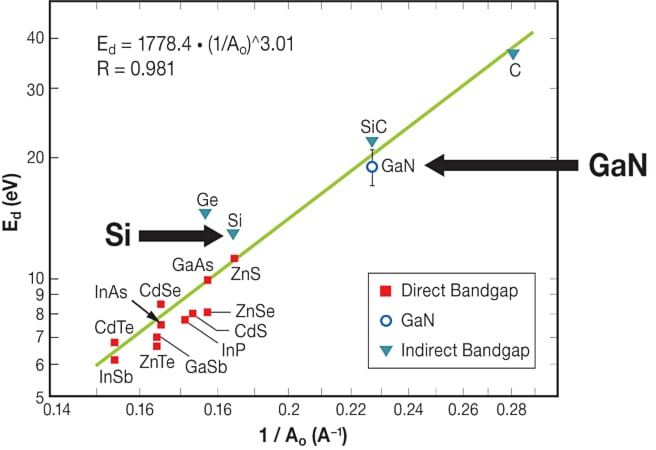
Figure 2. Displacement energy compared with the inverse of the lattice constant for various crystals(1). Image used courtesy of Bodo’s Power Systems [PDF]
Published reliability reports explain the failure mechanisms for GaN devices and establish predictive models so designers can estimate device lifetimes in their specific mission profile.
Beyond radiation resilience, GaN devices offer unmatched electrical performance compared to silicon MOSFETs. GaN devices enable power converters to operate at higher frequencies, resulting in greater efficiency and power density. For space applications like satellites and lunar habitats, this translates to smaller, lighter, and more efficient power supplies. GaN devices are significantly smaller and lighter, making them ideal for applications where space is at a premium. Their size reductions contribute to cost savings by optimizing space utilization in satellite payloads.
GaN Applications Transforming Space Missions
The advantages of GaN technology extend to various spaceborne systems:
- DC-DC Converters: GaN-based DC-DC converters, such as those used in satellite power supplies, offer peak efficiencies of up to 96%, outperforming silicon alternatives and contributing to increased energy efficiency in space missions.
- Lidar Systems: GaN’s speed and efficiency enhance lidar systems, providing higher resolution and more precise navigation for autonomous space missions and docking.
- Reaction Wheels: Critical for satellite orientation, GaN-powered reaction wheels offer precision control, reduced weight, and reliability in harsh space environments.
- Ion Thrusters: GaN enables smaller, lighter, and more efficient power supplies for ion thrusters, crucial for spacecraft propulsion and positioning.
GaN technology’s adoption in space missions has gained momentum, with collaborations between industry leaders like EPC Space and space agencies such as NASA, DLA, and ESA. These partnerships aim to standardize GaN technology testing and screening procedures, further validating its suitability for space applications.
The cost-saving potential of GaN technology is significant. Smaller power converters optimize space utilization, providing cost savings for satellite payloads. The efficiency improvements made possible by GaN translate to reduced power consumption and longer mission life. GaN’s robustness in harsh environments also minimizes component failures and replacements, contributing to sustainability by reducing electronic waste generated by space missions.
EPC Space: Rad-Hard GaN Transistors
EPC Space offers a family of rad-hard GaN transistors designed for radiation hardness. Every wafer is a radiation sample tested prior to shipping. These rad-hard GaN transistors offer ultra-low on-resistance and high current capability. These devices provide cost-effective, efficient, mission-critical components with a superior figure of merit, substantially smaller size, and lower cost than alternative rad-hard silicon solutions for satellite power supplies, robotic motor drives, instrumentation, reaction wheels, and deep space probes. EPC Space’s GaN devices have proven themselves with over 130,000 deployments in LEO and GEO orbits since 2017, solidifying their space heritage and reliability.
Gallium nitride (GaN) technology has ushered in a new era of power electronics in the space industry. Its resilience to radiation, superior electrical performance, cost-saving opportunities, and sustainability make it the go-to for space missions.
This article originally appeared in Bodo’s Power Systems [PDF] magazine.