Facebook
 Google
 GitHub
 Linkedin
Beyond Silicon: WBG GaN and SiC in Mature Markets
GaN and SiC technologies are being deployed across legacy silicon applications. What have we learned so far, and what’s to come?
While helping achieve CO2 reductions, electrification is driving up electricity demand. More loads are being connected to the grid simultaneously as applications demand more power to accomplish more complex tasks or, for example, charge batteries more quickly for vehicles. Design, cost, and legislative requirements combine to create a strong demand for greater efficiency, whether large appliances, computers, data center servers for AI processing, or chargers for devices such as power tools, domestic robots, e-bikes and scooters, and mobile phones.
In response to these pressures, wide-bandgap semiconductors that enable power supplies and converters to become more efficient and handle more power within the same or smaller footprint have become essential to modern designs. Both silicon carbide (SiC) and gallium nitride (GaN) technologies are commercialized and are already in products on store shelves and used in homes, offices, and factories worldwide.
SiC and GaN
SiC and GaN deliver superior switching performance in power transistors than legacy silicon. Faster transitions minimize power dissipation during turn-off and turn-on, resulting in greater efficiency and simplified thermal management. Faster transitions also permit increased switching frequency, thereby allowing the use of fewer and smaller passive components and associated savings in solution size and bill of materials. Smaller components and easier thermal management significantly reduce overall dimensions: greater power density equates to more power handling capability in a popular and established form factor or the same power and usefulness in a smaller form factor where desired. It’s also worth noting that fewer, smaller components add to the improved environmental sustainability that more efficient SiC and GaN technologies deliver thanks to ‘de-materialization’—the use of fewer materials and associated reductions in emissions from manufacturing and transport.
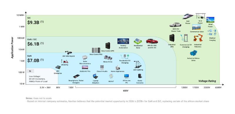
Applications for SiC and GaN technologies
While both display superior switching characteristics compared to silicon, each technology has individual strengths that can be used to delineate their applications. SiC has inherently higher thermal conductivity and a vertical device, which enables higher power density and dissipates heat more effectively. That’s why SiC is preferred in applications where high-voltage operation and heat dissipation (from high-power cycling) are priorities. These include electric vehicle inverters, industrial power supplies, solar-power designs, rail traction, wind turbines, grid distribution, and industrial and medical imaging.
GaN transistors can switch faster than SiC due to higher electron mobility and are therefore better suited to higher frequency applications in applications requiring voltages below around 650 V. As a result, GaN is more commonly used in soft-switching, high-power density power applications, including data center power supplies, electric vehicle charging, solar micro-inverters, and fast charging travel adaptors.
SiC Device Innovations
SiC MOSFET device designers have typically chosen a planar or trench gate architecture. Planar devices offer superior gate ruggedness and short-circuit capability with simpler manufacturing processing. On the other hand, trench architectures can offer superior on-resistance RDS(on) x area and RDS(on) x gate charge (QG) figures of merit.
Navitas’ patented trench-assisted planar-gate approach permits fast and cool operation with extended reliability while achieving high manufacturing yield by allowing simpler processing. These devices also have low RDS(on) at high temperatures and low energy losses at high speeds, boosting performance, robustness, and quality.
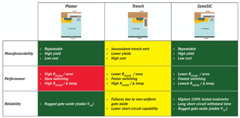
Comparison of conventional and trench-assisted planar architectures
RDS(ON) and temperature are particularly important. In datasheets, RDS(ON) is usually rated at 25°C, but depending on the temperature coefficient, this can significantly increase at elevated temperatures. The system’s ambient temperature can be up to 80°C, with device power cycling further elevating junction temperature. Navitas’ trench-assisted planar-gate SiC MOSFETs are designed with a very low RDS(ON) temperature co-efficient and have been shown to operate with a 25°C cooler case temperature than competing devices in experimental conditions. In practice, this 25°C equates to a three-fold increase in the device lifetime.
SiC Applications
In a domestic scenario, SiC devices bring valuable efficiency gains in solar inverters that convert DC power from a string of solar panels into grid-quality AC to be used immediately, stored, or supplied to the grid for a feed-in tariff. A small system may be rated for 4.6 kW AC. The electricity produced can be used immediately in the home, returned to the grid, or stored locally for later use.
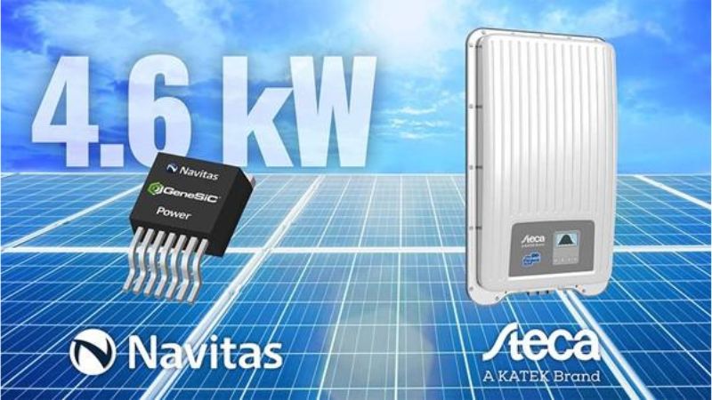
Companies use GeneSiC MOSFETs in their 4.6 kW ‘coolcept’ inverter topology to enable high peak efficiency results of 98.6%.
Navitas GeneSiC SiC MOSFETs have been chosen for a consumer-oriented 4.6 kW solar inverter, built with 16 MOSFETs, each rated at 1200 V and with 75 mΩ RDS(ON) and connected as a two-level H-bridge. This topology is inherently bidirectional, which eases integration with a domestic energy storage system. Because the SiC devices have significantly lower reverse recovery charge (Qrr) than silicon MOSFETs, the inverter can operate efficiently in reverse. SiC’s superior thermal performance ensures excellent reliability, while the technology also enables the inverter to operate at a relatively high switching frequency, permitting smaller passive components. This allows the enclosure to be smaller with a lower weight than conventional silicon-based inverters currently on the market.
GaN Devices and Applications
While SiC devices are typically selected for high-power, high-voltage applications, GaN technology is a strong choice for up to about 650 V applications.
Unlike silicon or SiC MOSFETs, GaN HEMTs have no body diode and completely eliminate any reverse-recovery issues. On the other hand, the HEMT gate structure is known to be sensitive. The device can be damaged if exposed to excessive gate-source voltage (VGS) overshoot, undershoot, or negative VGS spikes generated at low-side turn-off in high-power bridge circuits. There is also a high risk of unwanted turn-on that allows shoot-through currents to pass, and in buck circuits, the transistors can be vulnerable to drain-current surges.
Proper control of the gate is, therefore, vital for reliability as well as performance. Navitas GaNFast, GaNSense, and GaNSafe ICs ensure proper control by integrating a carefully designed gate driver in the package with the GaN HEMT. The driver uses optimized dead-time algorithms to prevent shoot-throughs, and the circuit layout ensures zero gate-source loop inductance. The devices can be switched safely at frequencies up to 2 MHz.
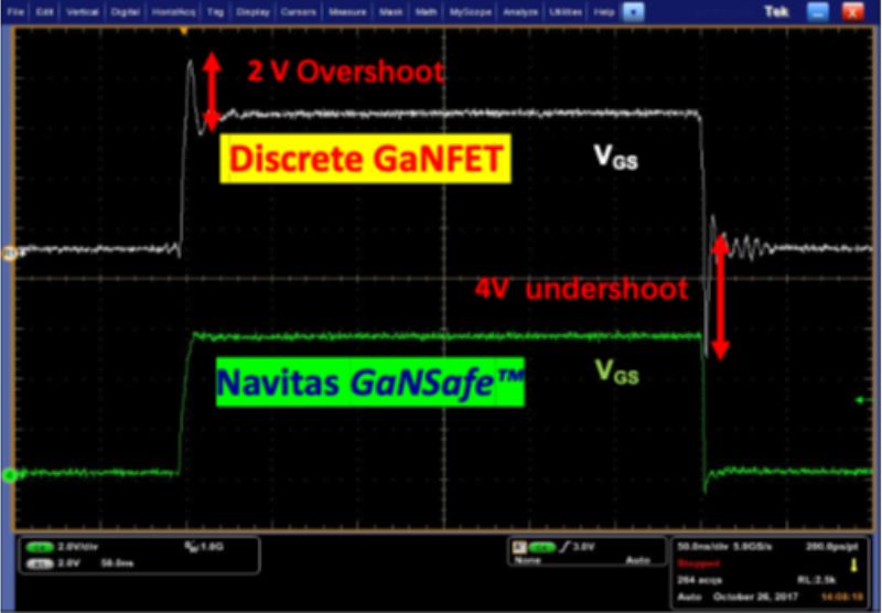
The GaNSafe gate driver eliminates the dangers of VGS overshoot.
Alongside the gate driver, the GaNSafe ICs also integrate protection and control circuitry to help save bill-of-materials costs, a Miller clamp that relieves any need for complex negative gate-voltage circuitry, and extra features for control and protection. These include dV/dt control at turn-on/turn-off, short-circuit protection with a response time of 300 ns, under-voltage protection, and thermal protection. There is also electrostatic discharge (ESD) protection up to 2 kV, typically not provided with discrete GaN transistors.
Navitas has created several reference designs based on its GaN and SiC technologies, including a 4.5 kW data center AI PSU in the industry-standard CRPS185 form factor. Optimized for high-performance computing (HPC) applications, including power for AI processing, this reference design exceeds 80Plus Titanium, the most stringent applicable eco-design standard. The PSU integrates boost PFC and an LLC resonant converter and has a 48 V output, enabling 137 W/inch^3 with over 97% efficiency, making it the highest power density AI PSU on the planet!
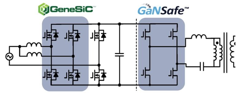
4.5 kW AI CRPS185 power supply reference design.
The Maturing WBG Market
Wide-bandgap devices are already widely adopted in applications across numerous markets, where high efficiency is required and reliability at high voltages and temperatures is expected. These range from data center power supplies, EV traction and OBC systems, and solar inverters to domestic equipment like chargers and appliance power supplies. Several generations of SiC and GaN devices have already been commercialized, and development continues, aiming to deliver even more robust and reliable devices to power-system designers.
The technology and markets for wide-bandgap power devices will continue to mature, particularly with GaN HEMTs, as devices have been in the marketplace for a shorter period than SiC MOSFETs. One notable observation is that the different gate designs can perform better with certain applications, such as motor controllers and power supplies. Recognizing this, Navitas continues developing devices that incorporate finely tuned properties for their target applications.