Facebook
 Google
 GitHub
 Linkedin
Analysis of Rad-Hard GaN Half-Bridge Power Stages for High-Rel Buck Converters
In this article, we analyze how monolithic GaN solutions and driver optimization maximize efficiency and power density in high-reliability space systems.
The aerospace industry is undergoing a technological transformation driven by the demand for more compact and efficient power systems. In this context, GaN has established itself as the natural successor to silicon, offering radiation hardness and superior switching capabilities at multi-megahertz frequencies.
This article analyzes how integrating isolated drivers and GaN HEMTs into half-bridge power stages maximizes energy density, overcoming traditional weight and volume limitations in high-reliability buck converters.

Figure 1. GaN technology is critical in high-reliability space system designs. Image used courtesy of Adobe Stock (licensed).
To delve deeper into these innovations, we feature exclusive insights from Bel Lazar, CEO of EPC Space, who emphasizes that the key to success in mission-critical applications lies in the adoption of monolithic solutions. According to Lazar, the ability of these platforms to mitigate EMI and optimize dead-time control not only simplifies the process for design engineers but also ensures exceptional thermal and electrical performance in the harshest environments of outer space.
High-Frequency Switching Theory and Driver Optimization
Dead-Time Setting
The EPC7C010 and EPC7C011 were configured to minimize the throughput delay mismatch of the low- and high-side power drivers. “In fact these drivers have functionally identical configurations,” Lazar added. “As shipped, the dead times for these two evaluation boards have a fixed 50ns dead time set by the input logic drive train.”
As can be seen in the scope capture of the switching node, for example as shown in Figure 2 for the EPC7C010 board, there is a fair amount of safety factor with the as-shipped dead time value(s).
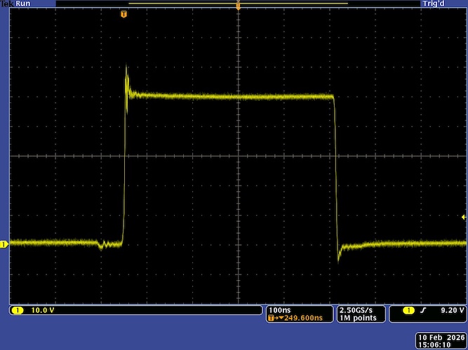
Figure 2. EPC7C010 evaluation board typical switching node waveform: VDD = 50 Vdc.
It is obvious that the low OFF to high ON switching node dead time is 45ns and the high OFF to low ON dead time is 60ns. These times include the transition times of the gate driver circuitry (NVE IL610CMTI and FBS-GAM01P-R-PSE).
“In the operating guide for the EPC7C010 it is recommended that the dead times be set to 25ns if lower 3rd quadrant losses are desired in the power HEMTs in the half-bridge,“ Lazar said. “That is the lowest value to use for a safety factor that accounts for tolerance and temperature effects.”
It should also be noted that both evaluation boards are shipped with anti-parallel Schottky diodes connected drain-to-source for each power HEMT in the half-bridge. The use of these diodes, along with a shorter dead time allows for even lower 3rd quadrant power losses. EPC Space Application Note AN009 offers a more detailed look at 3rd quadrant operation of an eGaN HEMT.
Throughput Delay Matching
To keep losses as low as possible as the switching frequency increases, it is imperative that a good degree of throughput delay time matching exists between the low- and high-side drivers. Obviously if the delay times are identical, the dead times may be set to a mínimum that guarantees that shoot-through/cross-conduction may not occur, with some DDED safety factor, to account for tolerances and temperature.
“Also, having the shortest throughput delay allows the switching frequency to be increased while having the ability to utilize a larger range of duty cycles from a given power driver,“ Lazar explained.
The duty cycle range is defined as the difference between the maximum and minimum duty cycles. We can calculate this range using the following equation:
$$\text{Duty Cycle Range} = \frac{(\frac{1}{f_s}) - 2\cdot t_{thru}}{(\frac{1}{f_s})}$$
where:
- fs is the operating frequency.
- tthru is the throughput delay mismatch between the high side and the low side of the driver, plus the deadtime.
As an example, let’s assume the following:
- fs = 2 MHz
- tthru= 50 ns
Substituting these values into the equation, we get:
$$\text{Duty Cycle Range} = \frac{(\frac{1}{2~E6}) - 2\cdot (50~E-9)}{(\frac{1}{2~E6})} =\frac{500~E-9~-~100~E-9}{500~E-9} = 80\%$$
For a duty cycle range of 80%, this means that the maximum duty cycle is 90%, and the minimum duty cycle is 10%.
At 3 MHz operating frequency, the duty cycle range becomes 70%, with a mínimum of 15% and a máximum of 85%. These values include dead times added by the control. So the possible duty cycle ranges only become smaller.
It can be seen that not only the throughput delay mismatch can have an effect on the possible operating duty cycle of the converter. “Couple this with the dead time and this further limits the operating duty cycle,“ Lazar added. “These limitations must be taken into consideration by the designer with regards to the intended application.”
PCB Layout Strategies for EMI and Thermal Management
High-Frequency EMI Mitigation
EMI is the manifestation of energy being diverted from an operating circuit by parasitic elements. Like displacement capacitance (think transistor package to heatsink capacitance) or stray loop inductance (think packaging inductance).
“In a half-bridge utilizing eGaN devices we care mostly about the parasitic magnetic loop area inductance. As the area of the current loop increases, so does the inductance,“ Lazar said. “So it benefits the designer to reduce the VDD-ground magnetic loop area that the high-frequency harmonics, caused by the rise/fall times, are routed through.”
Monolithic circuits are by their nature and construction physically smaller than their discrete counterparts. Their interconnections and semiconductor structures are smaller and closer together. Another consideration is the loop area in a discrete circuit includes the distance that the h/f current had to traverse in the Z axis—up from the PCB onto the discrete element and then down from the discrete element to the PCB.
And even though for eGaN devices the die to PCB interconnections are ball grid arrays, the current harmonics still have a finite Z axis path to traverse. So, for an equivalent performance monolithic circuit half-bridge, the parasitic inductance may be less than 50% of the discrete alternative.
The same rationale applies to the displacement capacitance as the smaller the overall die size, the lower the resultant die-to-plane parasitic capacitance will be. Smaller parasitic L and C elements carrying h/f current means smaller EMI emissions from the circuit, in general.
“As another example, notice the overshoot and h/f ring-out on the leading edge of the switching node, which is the result of the fast rise time of the half-bridge (5 ns) and the “un-cancelled” inductance of the VDD-to-ground power loop, including the decoupling capacitors. This is EMI,“ Lazar explained. “Rather, the amplitude of the undesired peak voltage and the ring-out frequency define the frequency spectrum of the unwanted EMI signal resulting from this overshoot.”
Obviously keeping the parasites in the circuit as small as possible keeps the extra noise that then needs to be contained or filtered at a mínimum. “Sweating the details” like reducing circuit parasitics can pay dividends in reducing the complexity of EMI filtering and packaging. This is especially important in space-based applications.
Decoupling Capacitor Placement
The most effective VDD-to-ground capacitor decoupling strategy is to place and connect the decoupling capacitors as close as possible to the VDD connection (the drain of the high-side power switch in the half-bridge).
Then an effective high-frequency ground return is created from the ground side of the decoupling capacitors to the ground connection (the source of the low-side power switch) using copper etch that mirrors the h/f current path in the top copper etch in the adjacent inner copper layer.
“This approach provides a great deal of magnetic flux cancellation in the PCB structure,“ Lazar added.
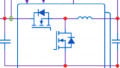
Figure 3 helps clarify the suggested layout technique to obtain magnetic flux cancellation.
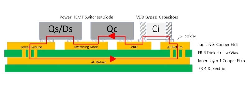
Figure 3. Decoupling and layout scheme to accomplish magnetic flux cancellation.
In Figure 3, the flux cancellation will (optimally) occur in parallel planes. When current transitions from the X-Y plane into the Z-direction (through vias and component leads), flux cancellation is incomplete. This is because the return path on the inner layer exists only in the X-Y plane, whereas the top-side path includes the vertical height of the components.
The top layer etch and the distance traversed into and from the components is slightly longer, and this slight difference in length evokes an associated (parasitic) inductance. A deeper dive into this topic may be found in EPC Space Application Note AN004.
System-Level Implementation in Aerospace Environments
Power Density Improvement
The controlling factor in increasing the operating frequency is the thermal penalty that is demanded from the power switches in the half-bridge, particularly with regards to the high-side switch. During switching operation, the high-side switch has to bear the full load current and full VDD voltage.
The power dissipated in a HEMT switch consists of three major parts: DC losses related to Rds(ON) and proportional to the duty cycle, AC losses proportional to Coss and switching losses proportional to the rise and fall times, and the switching frequency. So, for a fixed VDD, output current and rise/fall times, power losses will increase exponentially from any baseline with switching frequency.
“This means that the increase in switching frequency will have implications with regards to the power train in terms of the number of switches used in parallel to allow each switch to achieve the desired thermal objectives,” Lazar added. “If paralleling switches is not an acceptable situation, then the only way to resolve any thermal issues is to de-rate the operating criteria for the circuit.”
These two considerations, the necessity to either parallel switches or de-rate the VDD voltage and load current are the two factors from the power train perspective that affect the power density of the circuit. Otherwise, as the frequency increases, the inductor and capacitor values will decrease along with their physical sizes, allowing for an associated increase in power density.
As a general observation, this half-bridge solution will be more size efficient, and thus have greater power density, than competing solutions because it utilizes the eGaN HEMTs in the space-efficient “B” packaging, the FBS-GAM01P-R-PSE low-side gate driver module and the NVE IL-610CMTI GMR logic coupler (to achieve galvanic isolation for the high-side driver).
Because there are no rad-hard monolithic, isolated gate drivers at the 100 V+ operating level, the alternative is a transformer-coupled gate drive scheme which by the nature of the magnetics requires a larger physical footprint. Accordingly, both the EPC7C010 and 7C011 demonstrate the smallest possible footprint for a high-voltage half-bridge/non-isolated buck converter.
CMTI Performance
Given the observed rise times of the EPC7C010/011 evaluation boards, the circuits require common mode immunity to these switching transients of 20,000 and 40,000 V/µs, mínimum, respectively. With an added safety factor of 50%, those values become 40,000 and 80,000 V/µs.
“This means that the device utilized for the requisite galvanic isolation for the high-side must have these common-mode immunities at a mínimum. The logic isolator chosen, the NVE IL610CMTI has a mínimum guaranteed/tested CMTI of 100,000 V/µs,” Lazar said. “So this device provides the required transient immunity with the desired safety factor.”
Aside from the logic coupler, one has to be concerned with parasitic “displacement” capacitance from the high-side gate drive circuitry to ground. This capacitance can occur from plane overlaps of critical high edge-rate signals or improperly returned signals. The PCB layout for the EPC7C010/011 boards was carefully designed to create an isolated drive “islet” and return “planelet” for the high-side gate drive circuit.
The only, unavoidable, capacitance that exists from the gate driver circuitry to ground is that of the barrier capacitance (Cj) of the bootstrap diode used. And that diode is connected to the high-side 0.33uF bootstrap capacitor, so even though the transient causes 40mA peak current to flow in the Cj, this very short current transient accounts for less than 1mV of voltage sag on the bootstrap capacitor during the rise time event.
Accordingly, both the 7C010 and 7C011 boards are considered common-mode transient immune. Each board was operated with VDD 20% greater than the máximum level specified (120 and 240Vdc, respectively) and both boards operated as expected, thus demonstrating their robustness to fast induced transients.
The layout of the high-side gate driver circuit may be reviewed layer-by-layer in the Gerber PCB layer renderings included in the application guides for each board on the EPC Space website: ECP7C010 and EPC7C011.
A Leap Forward for High-Reliability Power Systems
The integration of monolithic GaN solutions and optimized driver configurations represents a significant leap forward for high-reliability power systems in aerospace applications. By leveraging the radiation hardness of GaN and minimizing parasitic elements through advanced PCB layout techniques—such as magnetic flux cancellation—designers can achieve unprecedented levels of efficiency and power density.
The transition from discrete to monolithic structures not only reduces the physical footprint of half-bridge stages but also significantly mitigates EMI, ensuring stable performance in the demanding environments of outer space.
Ultimately, successful implementation depends on a meticulous approach to circuit parasitics and thermal management. As switching frequencies reach the multi-megahertz range, the precision in managing throughput delays and CMTI becomes critical.
By "sweating the details" of the layout and adopting high-performance components like the NVE logic isolators and eGaN HEMTs, engineers can overcome the traditional trade-offs between size and reliability, paving the way for the next generation of compact, high-efficiency space-qualified buck converters.
All images used courtesy of EPC Space, except where specified otherwise.
Tony Marini, EPC Space
https://www.linkedin.com/in/tony-marini-85b5652/
EPC Space website https://epc.space/
eetech101
Anthony G.P. (Tony) Marini is an industry consultant at dtm Associates, Clinton, MA and Power Technologist at EPC Space, Andover, MA. He has over 45 years of industry experience in microelectronics, power circuits and semiconductor devices. He has over 15 years of experience using GaN and GaAs power devices. He has a BSEE and MSEE from Worcester Polytechnic Institute, Worcester, MA. He is a member of the IEEE and IMAPS.