Facebook
 Google
 GitHub
 Linkedin
A Simple, Effective Way to Suppress Voltage Spikes in Flyback Converters
Learn how to reduce voltage spikes in flyback converters using a low-cost, easy-to-implement clamping controller that improves efficiency and EMI performance without complex design changes.
Flyback converter topology is one of the most popular topologies adopted by low-power, isolated power supplies. The key to the flyback converter’s success is the ability to divide the buck-boost inductance into two windings of a transformer, creating flexible voltage and current ratios with the additional advantage of isolation. As a result, flyback converters require few components and achieve robust performance across a wide operating range.
However, critical voltage spikes result from the energy stored in the transformer’s leakage inductance, posing a common challenge in flyback converter design. Once the voltage spike exceeds the voltage rating, it can cause damage to the power switch. A secondary challenge caused by voltage spikes is electromagnetic interference (EMI), which introduces high-frequency harmonics.
Resistor-Capacitor-Diode (RCD) Snubber
Traditional solutions implement a passive resistor-capacitor-diode (RCD) snubber to absorb the leakage energy and mitigate the spikes. Figure 1 shows the conventional flyback circuit.
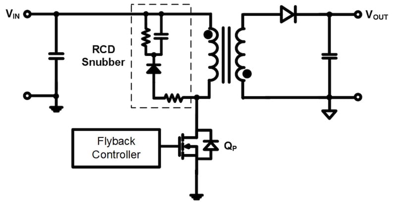
Figure 1. Conventional flyback circuit
Limitations of RCD snubbers include compromised efficiency performance as well as thermal issues that result from magnetizing energy consumption and expected leakage energy consumption. Reverse recovery of the diode in the snubber is also increasingly difficult to handle as the power increases. This limits the effectiveness of the snubber, sometimes even worsening oscillation in the converter. Therefore, a better solution for voltage spike suppression is necessary to design flyback converters with improved reliability, reduced EMI, and higher efficiency.
Active-Clamp Flyback (ACF)
In theory, the optimal solution can store all the leakage energy and cycle the energy back to the system without loss. This can be achieved with an active-clamp flyback (ACF) circuit that provides an additional active-clamping switch (QC) to replace the diode in the snubber (see Figure 2).
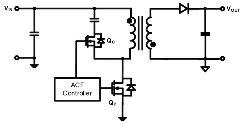
Figure 2. ACF circuit
With proper timing control over the on/off state of QC, the capacitance in the snubber can achieve well-controlled oscillation with the transformer’s inductance, eliminating the voltage spike. The leakage energy is also fed to the output through the oscillation.
ACF Circuit Limitations
Despite the advantages of active-clamp flyback (ACF) circuits and the availability of many ACF solutions on the market, the ACF controller has not been able to sufficiently replace conventional flyback converters, especially in high-voltage AC/DC applications, due to three key limitations:
- Increased cost of the main power device: The additional clamping switch (QC) in an ACF circuit is similar to (or sometimes exceeds) the main switch (QP) in terms of the voltage and on resistance characteristics, because the power is fully circulating in and out of QC. This doubles the cost of the main power device compared to the flyback converter.
- Increased cost of the ACF controller: The ACF controller is significantly more expensive than a flyback controller because of the additional high-side driver, more complex control scheme, and bigger IC package.
- High cost and risks of design changes: Implementing an ACF circuit changes the design in every aspect, including control, hardware, and debugging logic. Very few product designers are willing to transition from flyback to ACF, given the high costs and design risks.
Introducing a Clamping Controller Solution Using the HF300
To address voltage spikes in flyback controllers with minimal costs and design changes, MPS provides a clamping controller solution with the HF300 family. Figure 3 shows that the HF300 independently drives a clamping MOSFET (Q’C) by sensing the current flowing through Q’C, without requiring any communication to a primary flyback controller.
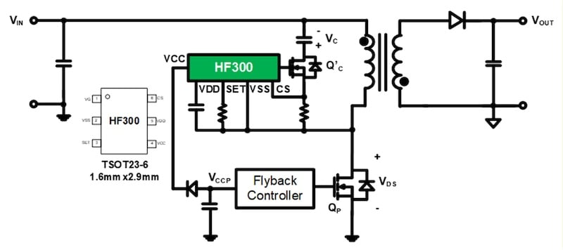
Figure 3. Conventional Flyback Controller Combined with the HF300
The HF300 is a 6-pin flyback controller IC in an ultra-small SOT23 package, with a body size that only spans 1.6mmx2.9mm. The additional MOSFET (Q’C) required by the HF300 is ultra-small as well, since only small leakage energy flows through Q’C. Overall, the HF300 offers lower cost, a smaller footprint, and minimal design changes mark notable advantages compared to an ACF solution.
Figure 4 shows the basic operating principles of the HF300. When the flyback’s primary switch turns off, the inductance current flows through the body diode of Q’C. The HF300 obtains the current measurements from the CS pin, and once the CS pin voltage (VCS) drops below the turn-on gate threshold (VCS_ON), the HF300 turns on Q’C. In this way, all the leakage inductance energy goes into the clamping capacitor, and the primary switch’s drain-source voltage (VDS) is sufficiently clamped at the sum of VIN and the clamping voltage (VC).
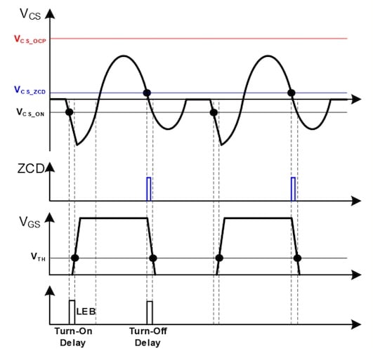
Figure 4. Operating principles of the HF300
During the turn-on phase of Q’C, the leakage inductor and the clamping capacitor oscillate with each other, and the HF300 continues monitoring the oscillating current through CS. As soon as VCS drops below the zero-current detection (ZCD) threshold (VCS_ZCD), the HF300 turns off Q’C. This means that when the resonant period is shorter than 4/3 of the minimum off time of QP, safe operation between QP and Q’C is guaranteed without any shoot-through. The required resonant period can be easily achieved by designing an appropriate clamping capacitance based on the leakage inductance.
Figure 5 shows experimental results based on a 65W AC/DC flyback power supply, comparing the impact of an RCD snubber and the HF300 on voltage spikes. With the RCD snubber, there is a voltage spike of 115 V. With the HF300, the spike voltage is reduced to 46V.
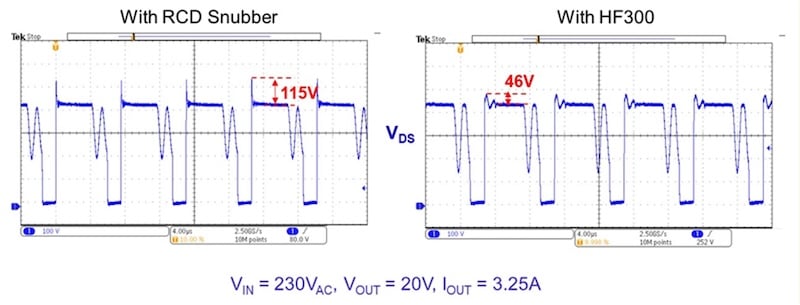
Figure 5. Experimental results comparing the impact of an RCD snubber and the HF300 on voltage spikes
Figure 6 shows the experimental results based on a 100W AC/DC flyback power supply, comparing the efficiency between the RCD snubber and the HF300. The HF300 shows a 0.3% efficiency improvement over the RCD snubber, especially at 115VAC.
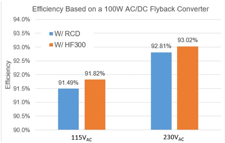
Figure 6. Experimental results comparing the efficiency between an RCD snubber and the HF300
These results demonstrate the ability of the HF300 to mitigate voltage stress in the flyback converter. At the same time, the lower peak voltage combined with the lower oscillation frequency improves EMI performance in the overall system. Figure 7 shows major improvements in the HF300’s EMI test results compared to the RCD snubber’s EMI test results, especially in the 1 MHz to 30 MHz range.
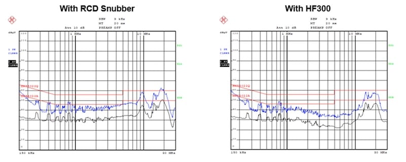
Figure 7. Experimental results comparing the emi between an RCD snubber and the HF300
Improvements Across the Board
This article discussed solutions for reducing voltage spikes in flyback converters with an RCD snubber, active-clamp flyback (ACF) circuit, and a clamping controller solution using the HF300. Among the existing solutions in the market, the HF300 can be substituted for a traditional RCD snubber in any existing flyback converter to significantly reduce voltage spikes without significantly changing the design or increasing the system cost. In addition, the HF300 also achieves improvements in EMI performance and efficiency.
To learn more, explore MPS’s secondary-side regulation solutions.
All images used courtesy of Monolithic Power Systems (MPS).