Facebook
 Google
 GitHub
 Linkedin
What are Enhancement-mode MOSFETs?
Learn about the principles of operation of p-channel and n-channel enhancement-mode MOSFETs.
Another structure used in making transistors is the enhancement-mode MOSFET. The enhancement-mode MOSFET is a widely employed field-effect transistor. Its structure is identical to the depletion-type MOSFET except that it has no built-in channel between drain and source. This device’s electrical characteristics are similar to those of the JFET and depletion-type MOSFET, but significant differences make it very interesting for many applications.

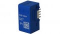
A 2N4351 enhancement-mode n-channel MOSFET. Image courtesy of Linear Systems.
Configuration of the n-Channel Enhancement-mode MOSFET (NMOS)
Figure 1 shows the structure of an n-channel enhancement-mode MOSFET.

Figure 1. n-channel enhancement-mode MOSFET.
A p-type substrate provides physical support for the device. Two heavily doped n-type regions make the source and drain. A thin layer of silicon dioxide (SiO2) – an outstanding electrical insulator – covers the area between the source and drain regions. Metal on top of the oxide layer shapes the gate electrode. The source, drain, and substrate, also known as the body, have metal contacts too.
Note the non-existence of a permanent channel between drain and source.
NMOS with Gate-to-Source Voltage Vgs = 0
Usually, the p-type substrate and source terminals are connected. In this way, the substrate won’t affect the device’s operation, and the MOSFET will work as a three-terminal device.
If the gate is also connected to the source so that there is no potential difference between the gate and the substrate, no current can flow between drain and source. Regardless of the voltage polarity from drain to source, there is always a reverse-biased junction (diode) either at the drain or the source – one diode by the p-n junction between the n-type drain region and the p-type substrate, and another diode by the p-n junction between the p-type substrate and the n-type source region. These two back-to-back diodes block the current flow – very different from the JFET and depletion-type MOSFET where Id = Idss (saturated short-circuit drain current) when Vgs = 0.
The definition of Idss has no meaning in an enhancement-mode MOSFET because Id = 0 A when Vgs = 0 V.
The considerable accumulation of free carriers (electrons) at the drain and the source (due to the n-doped regions) is useless without a path between them – the route between drain and source has a very high resistance.
In conclusion, with no voltage applied to the gate, the transistor is an open circuit between drain and source.
NMOS with Gate-to-Source Voltage Vgs > 0
The voltage applied to the gate regulates the current flow between the source and drain.
Giving Vgs a small positive value, the positive charge on the gate repels the free holes in the substrate under the gate, entering deeper regions of the p-substrate and forming a carrier-depletion region near the SiO2 insulation layer between drain and source.
The bound negative charge related to the acceptor atoms occupies the carrier-depletion region. These charges are “uncovered” because the neutralizing holes are driven into the substrate.
Making the gate more positive, the charge on the gate attracts free electrons into the carrier-depletion region from the n-type source and drain regions (where there are plenty of them). The electrons accumulated induce an n-type channel at the oxide-silicon interface, connecting the drain and the source, as seen in figure 2.

Figure 2. Channel formation in the enhancement-mode NMOS.
A current can now flow through the transistor, applying a voltage between drain and source. This current will flow from drain to source through the induced n-type region, carried by the free electrons.
Another name for the induced channel is the inversion layer – because of its creation by inverting the substrate surface from p-type to n-type.
Figure 2 also shows the parallel-plate capacitor formed between the gate and the channel – with the SiO2 insulation layer working as a dielectric – the positive charges that accumulate on the top plate, caused by the positive Vgs, and the resultant negative charge created by the electrons in the channel.
An NMOS is a field-effect transistor (FET). Accordingly, an electric field develops in the capacitor to control the number of charges in the channel, its conductivity, and the magnitude of the current flowing.
The threshold voltage VT is the Vgs voltage at which the channel forms. The magnitude of the threshold voltage depends on the substrate’s electrical properties and the oxide properties and thickness. For an NMOS, VT is a positive value.
The device’s manufacturing process controls the value of VT, and it appears as Vgs(Th) on the specification sheets.
The current Id = 0 A when the gate voltage is less than the threshold voltage because no channel exists under this condition.
Increasing the gate voltage above VT induces more free electrons into the channel, decreasing its resistance. Then, the device acts as a voltage-controlled resistor. When the channel is pinched off the MOSFET acts as a voltage-controlled constant current device.
NMOS with Gate-to-Source Voltage Vgs < 0
The gate voltage of a depletion-type NMOS or JFET can deplete or enhance the concentration of free carriers in the channel, depending on whether Vgs is negative or positive. The gate voltage of an enhancement NMOS can only enhance the concentration of free carriers in the channel – the transistor only works in enhancement mode (Vgs > 0). This condition is the basis to name the device enhancement-mode MOSFET.
Applying a Voltage Between Drain and Source
The minimum voltage required to maintain the induced channel is the threshold voltage VT. Having an induced channel and making the drain positive relative to the source, causes the flow of a current Id. The free electrons travel from source to drain, and the current Id direction is from drain to source, as seen in figure 2. Due to the high input impedance, the gate current Ig = 0 A.
The channel is not pinched off when the drain-to-source voltage is small, and the NMOS behaves as a linear resistor with a value controlled by Vgs.
Increasing the drain-to-source voltage triggers pinch-off at the drain side of the channel just as it does in the depletion-type NMOS and JFET.
Pinch-off takes root at the drain side of the channel when
Vgd = VT > 0 (1)
But Vgd = Vgs – Vds (2), then
Vgs – Vds = VT > 0 (3), or
Vds = Vgs – VT > 0 (4).
The channel is not pinched off when Vds is less than the value in equation 4.
Keeping Vgs constant and increasing Vds, the drain current will ultimately reach a saturation level. For example, keeping Vgs in equation 2 fixed at some value, say 8 V, and increasing Vds from 2 V to 5 V, Vgd will decrease from 6 V to 3 V. It means that the gate becomes less positive with respect to the drain.
This gate-to-drain voltage reduction will lessen the attractive forces for free carriers – electrons – in this induced channel region and diminish effective channel width. Eventually, increasing Vds will reduce the channel to the pinch-off point, establishing a saturation condition – the NMOS enters the saturation region or the saturation mode.
When Vds increases above the pinch-off value, the voltage drop along the channel stays constant at the Vds value of equation 4. The drain current Id is also constant (at saturation level), no matter the magnitude of Vds. Therefore, both the voltage drop across the channel and the current through it remain constant in saturation.
Channel pinch-off does not mean channel obstruction – the current continues flowing through the pinched-off channel.
The Drain Characteristic and the Transfer Curve of the NMOS
Figure 3 shows an example of drain characteristics for an enhancement type NMOS. The volt-ampere characteristics for the enhancement-mode NMOS have the same form as the FET characteristics.

Figure 3. Drain characteristics for an enhancement-mode NMOS.
Note that the resistance in the ohmic region is infinite for Vgs ≤ VT and decreases as Vgs increases. Although Vgs is the parameter for the characteristics in figure 3, they depend on Vgs - VT – the effective voltage or overdrive voltage.
Equation 4 exhibits the relationship between the saturation level for Vds and the magnitude of Vgs. For a set value of VT, the higher the level of Vgs, the greater the Vds value that causes saturation.
Figure 3 shows that the saturation portion of the drain characteristics is a horizontal straight line. The saturation level for Id increases as Vgs rises, starting from a value VT to + 6 V. Note that the spacing between the levels of Vgs increases as the voltage increases, resulting in growing increments in drain current. The drain current Id of an enhancement-mode NMOS is 0 A for values of Vgs < VT.
Extending the drain characteristics to sufficiently high drain voltages triggers channel breakdown. This failure results from avalanche breakdown in the space-charge region at the drain side of the channel.
Figure 4 shows the transfer characteristic for an enhancement-mode NMOS.

Figure 4. Transfer curve for an enhancement-mode NMOS.
When Vgs > VT, Id, and Vgs are related by the nonlinear relationship
Id = k(Vgs - VT)² (5)
Where the constant k depends on the device’s physical characteristics.
The transfer curve for an enhancement-mode NMOS is totally in the positive Vgs region and starts rising at Vgs = VT.
The transfer curve follows the saturation levels of the drain characteristics. Consequently, the region of operation is for Vds values greater than the saturation levels defined by equation 4.
Configuration of the P-Channel Depletion-mode MOSFET (PMOS)
An enhancement-mode PMOS is the reverse of an NMOS, as shown in figure 5. It has an n-type substrate and p-type regions under the drain and source connections. Identifying the terminals is the same as in the NMOS but with inverted voltage polarities and current directions. The NMOS and PMOS are complementary transistors.

Figure 5. Channel formation in the enhancement-mode PMOS.
A negative voltage applied between gate and source induces a p-channel – with p-type carriers – allowing the current flow between the source and drain. An electric field is directed perpendicularly through the oxide that ends on the induced positive charges on the semiconductor side. The positive charges – the minority charges in the n-type substrate – form an inversion layer.
The Drain Characteristic and the Transfer Curve of the PMOS
Figure 6 shows the drain characteristics of an enhancement-mode PMOS.

Figure 6. Drain characteristics for an enhancement-mode PMOS.
Increasing the magnitude of the gate-to-source negative voltage raises the induced positive charges in the semiconductor and the conductivity of the region beneath the oxide. Thus, the negative gate voltage enhances the drain current Id.
Figure 6 shows that the current Id rises slowly at first and then much more rapidly with increasingly negative values of Vgs.
Figure 7 shows the transfer curve of an enhancement-mode PMOS.

Figure 7. Transfer curve for an enhancement type PMOS.
This transfer curve is the mirror image of the transfer curve of figure 4, with Id increasing with ever more negative values of Vgs exceeding VT.
About Enhancement-mode MOSFETs
The enhancement-mode MOSFETs have small geometry, low power dissipation, and ease of manufacture. These features make them suitable for use in integrated circuits.
There is no path between the drain and source when no voltage is applied between the gate and source terminals.
Applying a gate-to-source voltage enhances the channel, making it capable of conducting current. This attribute is the reason to label this device enhancement-mode MOSFET.
Enhancement-mode MOSFETs only operate in the enhancement mode, unlike the depletion-type MOSFETs that operate in enhancement and depletion modes.
Applying a positive gate-to-source voltage to an NMOS creates an n-type channel layer allowing the free carrier’s conduction from source to drain.
The threshold voltage VT is the gate-to-source voltage that starts to form the drain-source channel. When Vgs is less than VT, the drain-source channel doesn’t exist, and the drain current Id = 0 A.
The magnitude of VT depends on the device’s construction characteristics, with a particular value for every MOSFET.
The quantity Idss found in JFET, and depletion-type MOSFETs is not appropriate to the enhancement-mode MOSFET since Id = 0 A when Vgs = 0 V.
In an enhancement-mode PMOS, a negative Vgs creates a p-type channel layer that transmits free carriers from source to drain.