Facebook
 Google
 GitHub
 Linkedin
Taking Power Conversion to the Next Level
Multi-level buck conversion is not new and has been applied in higher voltage and power devices for years. The need for high power delivery in small, low-profile applications such as smartphones makes multi-level uses attractive.
This article is published by EEPower as part of an exclusive digital content partnership with Bodo’s Power Systems.
While multi-level buck conversion has been applied in higher voltage and power devices for many years, the need for high power delivery in small, low-profile applications such as smartphones makes multi-level uses attractive.
Many mobile electronic products require lower-profile form-factor solutions with increasing power requirements. This is especially true for consumer and mobile devices such as low-profile smartphones and tablets—sometimes described as a 3D jigsaw puzzle of PCB boards, antennae, and interconnects. Meanwhile, battery charging speeds are continually increasing, and core processors march toward finer-geometry silicon with low-voltage supply requirements and increasing currents.

Image used courtesy of Adobe Stock
Traditionally, power conversion has been based on the step-down buck converter shown in Figure 1 (i). The buck architecture is commonly used and well-understood but has limitations. If we consider the switch node as the midpoint of the buck FETs, this node switches between the entire input voltage and ground. This means that the output filter—the output inductor and capacitance—must be relatively large, which is problematic for low-profile applications.
To solve the issue, we believe that the answer is to take power conversion to the next level and introduce the concept of multilevel power conversion. The multi-level buck converter shown in Figure 1(ii) (in this case, 3-level) is closely related to the traditional buck converter but expands the number of switching levels. Hence, there is a level of familiarity for designers and customers alike. The topology is not new and has traditionally been used in higher input voltage and higher power applications. However, the ability to reduce the size and height of the output inductance and achieve high levels of conversion efficiency makes the topology more attractive to lower-voltage applications with demanding low-profile requirements.
As always, any advanced architecture presents challenges. The increased number of switches increases the complexity of the control and gate drive circuity. This article addresses some of the advantages and resolutions to some of the challenges before providing some real-product performance measurements and data.

Figure 1(i). Buck Converter. Image used courtesy of Bodo’s Power Systems [PDF]

Figure 1(ii). 3-Level Buck Converter. Image used courtesy of Bodo’s Power Systems [PDF]
Multi-level Basics: Buck vs. Multi-level Buck Conversion
The traditional buck converter shown in Figure 1(i) is widely used but carries some limitations. The buck topology can be considered as a 2-level buck converter with the switch node (center point of the switching FET) switching between two levels: input voltage and ground (or approximately one diode drop below). This means that the switch node waveform sees a significant voltage excursion which requires a large output filter —output inductor, and output capacitor—to provide a smooth DC voltage to the output load. The voltage stress is further increased by leakage and parasitic inductances as the current reverses in the output inductor. The net result is that the designer must select higher-voltage FETs, reducing the conversion efficiency.
The multi-level buck converter has several benefits over a standard buck converter. Figure 1(ii) shows a 3-level buck converter. The name of the converter derives from the switching node of the inductor switching between three levels. In a buck converter, the inductor switching node switches between input voltage and ground, or two levels. But in the 3-level buck, the inductor’s switching node can switch between either the input voltage, ground, or half of the input voltage.
The extra switching states offer some big advantages. The frequency seen across the inductor is twice the frequency of the switching MOSFETs, resulting in a smaller inductor. In a standard buck, the voltage seen across the inductor in the charging state is VIN-VOUT. But in 3-level, it is ½ VIN-VOUT, yielding a lower inductor ripple current.
In a typical buck converter, the voltage seen across the MOSFETs is VIN. But in a 3-level buck, the voltage is ½ VIN. To take advantage of this, lower-rated MOSFETs are used. The Rds_on of the MOSFET roughly scales with the voltage rating squared. The lower voltage rating of the MOSFETs can have ¼ the Rds_on in the case of a 3-level buck.
Figure 2 shows the four possible switching states of the 3-level buck for continuous conduction mode operation. During steady-state operation, the inductor switching node switches between two voltages, like a standard buck. When the output voltage is above ½ the input voltage, states 1, 2, and 3 are used. When the output voltage is below ½ the input voltage, states 2, 3, and 4 are used.
States 2 and 3 keep the voltage balanced on the fly capacitor, C1. To keep the voltage balanced, the voltage across the fly capacitor is monitored. The voltage is actively balanced by the control loop.
Figure 3 shows the 3-level buck inductor current and the inductor switching node voltage in continuous conduction mode and when VOUT < ½ VIN. As discussed, in the 3-level buck, the switch node switches between ½ VIN and GND. During the inductor charging, either state 2 or 3 is used. The PWM controller logic chooses state 2 or 3 depending on the fly capacitor voltage. If the fly capacitor voltage is too low, state 3 is chosen. If the fly capacitor voltage is too high, state 2 is chosen. This keeps the voltage on the fly capacitor at ½ VIN.
Figure 4 shows the 3-level buck inductor current and the inductor switching node voltage in continuous conduction mode and when VOUT > ½ VIN. States 2 and 3 are used again to balance the voltage on the fly capacitor.
Moving to the Next Level
By adding more MOSFETs and fly capacitors, the 3-level buck converter can expand to 4 levels or more. A major benefit of adding more levels is to reduce the voltage stress on the MOSFETs. With a 3-level buck, the MOSFETS see one-half the input voltage. With a 4-level buck, the MOSFETs see one-third the input voltage. With a 5-level buck, the MOSFETs see one-quarter the input voltage, and so on. In an N-level buck converter, the MOSFET voltage is reduced to 1/ (N-1). These higher multi-level buck converters, shown in Figure 5, have an advantage in high input voltage applications with lower-rated MOSFETs and lower switching losses.

Figure 2. 3-Level Buck Switching States. Image used courtesy of Bodo’s Power Systems [PDF]

Figure 3. 3-Level Buck Steady-State Waveforms when VOUT < ½ VIN. Image used courtesy of Bodo’s Power Systems [PDF]

Figure 4. 3-Level Buck Steady State Waveforms when VOUT > ½ VIN. Image used courtesy of Bodo’s Power Systems [PDF]
Figure 5 (ii) illustrates a 4-level buck converter. The 4-level buck converter adds two MOSFETS and one fly capacitor to the 3-level buck. With more MOSFETs and now four levels, the 4-level buck converter has eight different possible switching states.
Again, as in the 3-level buck, the fly capacitor voltages require active balancing. The voltage on each fly capacitor is monitored. When the input is below one-third the output voltage, the inductor switching node switches between 0 and 1/3 VIN. To keep the fly capacitors balanced, the PWM controller cycles between states 2, 3, or 4 as shown in Figure 6.
In applications that require wide-range input voltages, we can run at four levels for high input voltage ranges and switch to three levels for mid-to-low input ranges by shorting out a level of switches and optimizing the conversion efficiency. This can be particularly useful for USB input equipment which can range from 5 V to 20 V. Shorting the fly capacitors together by leaving Q2 and Q5 permanently on turns the 4-level converter into 3-level converter, as shown in Figure 7.

Figure 5 (i). 3-Level Buck Converter. Image used courtesy of Bodo’s Power Systems [PDF]

Figure 5 (ii). 4-Level Buck Converter. Image used courtesy of Bodo’s Power Systems [PDF]

Figure 5 (iii). N-Level Buck Converter. Image used courtesy of Bodo’s Power Systems [PDF]
Hybrid Conversion
In general, an unregulated charge pump or switching capacitor converter offers better efficiency than a traditional regulated buck converter. Note that a multi-level converter can be transformed and operated as a charge pump. For example, the 3-level buck converter can be configured to operate as a divide-by-2 charge pump using the same FET structure.
Figure 8 shows a (i) divide-by-2 charge pump compared to a (ii) 3-level buck. The inductor in the 3-level buck converter is required for regulation. Removing the inductor in a 3-level buck converter transforms it into a divide-by-2 charge pump. Charge pumps usually do not require an output inductor to operate.

Figure 6. 4-Level Buck Switching States. Image used courtesy of Bodo’s Power Systems [PDF]

Figure 7. 4-Level Buck Transition to 3-Level Buck. Image used courtesy of Bodo’s Power Systems [PDF]
However, pSemi has developed charge pump architectures that use a small, adiabatic output inductance. Adding an inductor can eliminate the charge redistribution loss in the fly capacitor. In a charge pump, a capacitor is typically switched in parallel or series with other capacitors resulting in charge redistribution loss. An adiabatic inductor allows the current to resonate between capacitors, eliminating the charge redistribution loss and improving charge pump efficiency.
This scheme can be employed if the output inductor is small enough to satisfy the adiabatic performance of the charge pump. The multi-level converter can achieve lower output inductance for the reasons mentioned previously. Hence, the architecture can be switched between multi-level mode and charge pump mode to form an adaptable hybrid converter.
By switching from 3-level buck operation to charge pump operation, we keep the buck inductor in series with the output. The control is changed from a standard PWM control in 3-level buck mode to charge pump control. In charge pump control (see Figure 2), the fly capacitor, C1, voltage is monitored. Switching states 2 and 3 are used. When the fly capacitor voltage is too low, the controller switches to state 3. When the fly capacitor voltage is too high, the controller switches to state 2.
Similarly, the 4-level buck converter can operate as a divide-by-3 charge pump. Figure 9 shows a divide-by-3 charge pump and 4-level buck converter. In charge pump mode, both fly capacitors are monitored to maintain the correct voltages on each capacitor. States 2, 3, and 4 keep C1 charged at one-third of the input voltage and C2 at two-thirds of the input voltage.
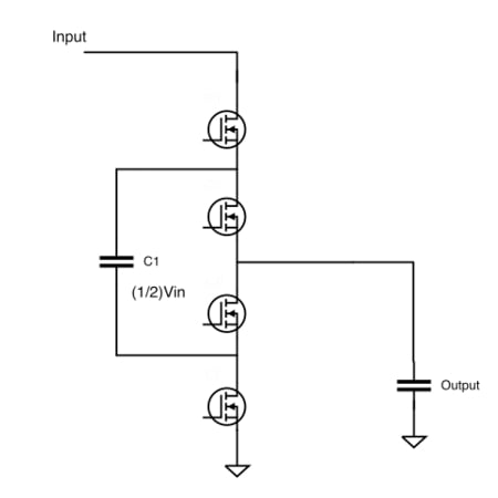
Figure 8 (i). Divide-by-2 Charge Pump. Image used courtesy of Bodo’s Power Systems [PDF]
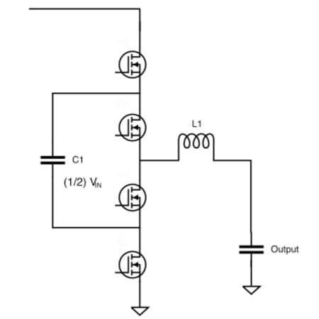
Figure 8 (ii). 3-Level Buck Converter. Image used courtesy of Bodo’s Power Systems [PDF]
When operating in charge pump mode, the 4-level buck inductor is in series with the charge pump output. Because the switching node has small ripple, the inductor ripple current is very small. The inductor performs the adiabatic function in divide-by-3 as in divide-by-2 described earlier.
From Theory to Practice
This section shows real waveforms from a multi-level converter capable of operating over a wide input range 4.5V to 18V. The device can operate in 4-level mode buck mode, generally used at higher input voltages, and in 3-level buck mode, generally for mid-to-low input voltages. As described in the previous section, the device can be operated in charge pump, capacitor divider mode with divider ratios 2 and 3. Current delivery is up to 6A in all modes using a 1 mm height inductor.
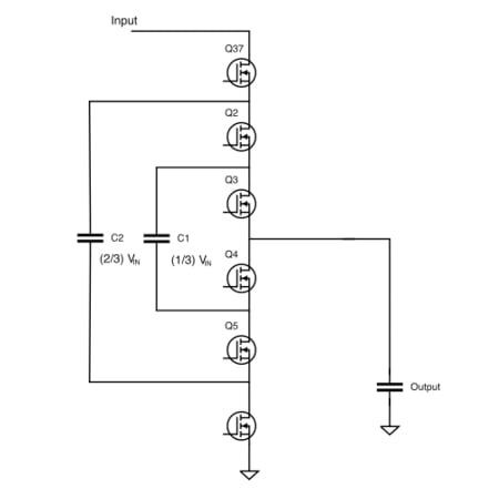
Figure 9 (i). Divide-by-3 Charge Pump. Image used courtesy of Bodo’s Power Systems [PDF]
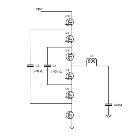
Figure 9 (ii). 4-Level Buck Converter. Image used courtesy of Bodo’s Power Systems [PDF]
Figure 10 shows operation in 3-level mode. In Figure 10 (i), the VIN to VOUT ratio is less than 0.5. Hence, the FET/inductor node switches between 0 and ½ * VIN. In Figure 10 (ii), VIN is reduced to 6V. Now the VIN to VOUT ratio is greater than 0.5. So, the device switches between ½* VIN and VIN.
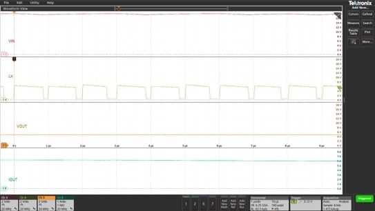
Figure 10 (i). 3-Level -lower half: 12VIN with 4.5VOUT Switching node moves between 0 to ½*VIN. Image used courtesy of Bodo’s Power Systems [PDF]

Figure 10 (ii). 3-Level -Upper half: 6VIN with 4.5VOUT Switching node moves between ½*VIN to VIN. Image used courtesy of Bodo’s Power Systems [PDF]
Figure 11 shows the device operating in 4-level mode with the input voltage changing from (i)18V to (ii) 12V and then to (iii) 6VIN input. This exercises the converter at each level, but in all instances, we can see that the voltage excursion on the switch node is always one-third of the input voltage.

Figure 11 (i). 4-Level - lower third: 18VIN with 4.5VOUT Switch node moves between 0 to 1/3* VIN. Image used courtesy of Bodo’s Power Systems [PDF]

Figure 11 (ii). 4-Level – middle third: 12VIN with 4.5VOUT Switch node moves between 1/3* VIN to 2/3 *VIN. Image used courtesy of Bodo’s Power Systems [PDF]
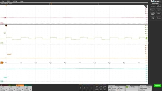
Figure 11 (iii). 4-Level -Upper third: 6VIN with 4.5VOUT Switching node moves between 2/3*VIN to VIN. Image used courtesy of Bodo’s Power Systems [PDF]
Conclusions
The concept of multi-level buck conversion is not new and has been applied in higher voltage and power devices for many years. However, the need for high power delivery in small, low-profile applications such as smartphones makes multi-level uses more attractive. The topology provides many advantages, resulting in smaller, lower-profile output inductors and the use of lower voltage FETs for higher efficiency. As with all advanced power architectures, there are added complexity and control techniques that must be applied, but problems such as dead-zone operation and fly-capacitor balancing are solvable.
The multi-level approach is particularly appealing in smartphone applications where solutions are expected to be <1 mm in height. The topology can provide high efficiency and high-power delivery to increase battery charging speeds and provide high current supply to sub-10 nm processor ASICs that demand higher currents at lower supply voltages.
One key challenge facing the smartphone industry is supporting a plethora of new and legacy ‘wired’ and ‘wireless’ charging voltage requirements. The multi-level approach can adapt and transform depending on the type of input voltage presented. If the input adapter is fixed to USB_PD (power delivery), it is enabled as a multi-level buck converter. Depending on the input voltage magnitude, this could be implemented as a 4-level, 3-level, or 2-level. If the adapter type is PPS and presents a variable input voltage, the multi-level converter can act as a capacitor divider charge pump. Truly, this is an intelligent hybrid architecture.
pSemi-Murata has developed the industry’s first multi-level converter capable of operating to four levels and as a charge pump capacitor divider capable of delivering high current. pSemi will showcase a hybrid 4-level buck and charge pump converter for power conversion in mobile platforms for the first time at APEC 2025 this week. Based on a substantial body of IP developed over the last 13 years and originating from patents from MIT, pSemi is now able to demonstrate products that take power conversion to the next level.
This article originally appeared in Bodo’s Power Systems [PDF] magazine and is co-authored by Laurence McGarry, Director of Product Line Management, and Doug Osterhout, Applications Engineer, pSemi Corporation.