Facebook
 Google
 GitHub
 Linkedin
Reports of Silicon’s Death Have Been Greatly Exaggerated
Learn how a new MOSFET architecture stretches the performance of silicon power devices using a patented approach.
This article is published by EEPower as part of an exclusive digital content partnership with Bodo’s Power Systems.
Silicon remains the backbone of the power semiconductor industry due to its mature manufacturing base, cost structure, and reliability. However, in recent years the industry has only seen incremental improvements in silicon power technology. The last significant breakthrough took place in 1998 with the commercialization of Superjunction devices, more than 25 years ago.
SuperQ is a new MOSFET architecture that extends the performance of silicon power devices within this established framework. It uses a novel, patented asymmetrical reduced surface field (RESURF) structure that significantly increases the n-conduction region of the device – up to 95% of the conduction area versus 50% or less in traditional Superjunction and other RESURF technologies.
This structural shift enables notable reductions in on-resistance (RDS(on)) and switching losses while maintaining the proven advantages of silicon: low cost, high-volume manufacturability, and robust reliability.
Commercialization of devices based on this technology began in July 2025, with iDEAL Semiconductor launching an initial product lineup including both 150 V and 200V MOSFETs, which are in full production. High-voltage offerings, from 250 V to 400 V, are in development as part of the near-term roadmap.
SuperQ is positioned for applications where silicon’s cost and availability are critical but where performance headroom is still required – such as motor drives, AI datacenter power delivery, telecom, and other high-efficiency power conversion systems. In this article, we’ll examine how the technology enables these advances in Cost x Performance versus legacy silicon devices.
SuperQ Technology: Architectural Benefits
To better understand SuperQ, it’s essential to trace the evolution of power semiconductor architectures, starting with 1979’s “HEXFET” MOSFET. This structure utilized 100% of the silicon area for conduction but suffered from quadratic resistance increases at higher voltages, which significantly impacted efficiency (see Figure 1).
In 1998, RESURF architectures, more commonly referred to as “Superjunction,” were commercialized. This technology introduced 2-dimensional charge balancing, which allowed for higher voltage blocking (BV) and resistances that scaled almost linearly with BV. However, these architectures dedicate only about 50% of the die to conduction, with the remaining P-regions only supporting voltage blocking (see Figure 1). Performance in these devices is plateauing as the architectures reach manufacturing limits with correspondingly higher costs.
As a result, the industry steered research dollars towards alternative, wide-bandgap (WBG) materials like silicon carbide (SiC) and gallium nitride (GaN). These semiconductor technologies gave further gains but came with significantly higher costs as well as manufacturing complexities, long-term reliability risks, and implementation challenges.
Unlike Superjunction architectures, SuperQ uses an asymmetrical RESURF structure (see Figure 1). Further gains in performance are achieved by widening the silicon’s N-conduction regions. SuperQ replaces Superjunction’s P-pillar with a proprietary, patented high aspect ratio deep trench with sidewall charge. The technology achieves voltage blocking at 19–20 V/μm and enables thinner epitaxial layers with higher doping profiles.
This results in a dramatically lower specific on-resistance (Rsp), which is 2.6x better than traditional silicon at 200 V, without departing from silicon’s mature ecosystem (see Figure 2).
The design also leverages a simple, CMOS-compatible manufacturing flow on high-volume 200 mm or 300 mm wafers, ensuring high yields and compatibility with existing fabs.
Unlike SuperJunction’s complex epi+implant process, SuperQ is optimized for performance and cost. The platform is scalable across diodes, MOSFETs, IGBTs, and power ICs and can be used for voltages from 60 V to 1,200 V, with potential extensions to future alternative semiconductor materials when they are commercially viable.
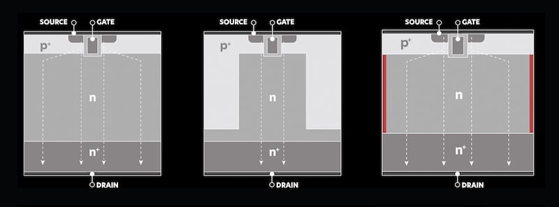
Figure 1. Evolutionary diagrams of MOSFET structures, showing SuperQ’s asymmetrical design (right) versus conventional HEXFET (left) and Superjunction (middle). Image used courtesy of Bodo’s Power Systems [PDF]
Performance Metrics and Benefits
SuperQ offers improved performance through measurable gains in silicon MOSFET figures of merit (FOM). Its architecture optimizes the conduction area, resulting in a significant reduction in on-resistance. For instance, the 150 V technology scales as low as 2.5 mΩ in a TOLL package, which is equivalent to the industry leader and 1.6x lower than the next best competitor.
At 200 V, iDEAL is capable today of 3.7 mΩ in a TOLL – almost half of the industry leader and 2.6x lower than the next best competitor. At 400 V, capabilities in a TOLL package extend not just below silicon but the industry’s lowest silicon carbide device at 400 V.
Beyond conduction, switching metrics stand out. Switching charge (QSW) is reduced by up to 2.1x compared to leading competitors (see Figure 3). This parameter, proportional to switching time, minimizes losses as shown by the formula for half-cycle switching loss.
\[P_{SW}=\frac{1}{2}*V*I*\frac{Q_{SW}}{I_{G}}*F_{SW}\,\,\,\,\,(1)\]
As a result, SuperQ devices can switch up to 2.1x faster or save the equivalent power losses, supporting higher frequencies in demanding topologies. The device also stores less energy in the device’s Output Capacitance (COSS). Compared to silicon competitors, it is up to 4.4x lower. Even compared to industry-leading GaN devices, capacitive stored energy (EOSS) is cut in half (see Figure 3).
\[P_{EOSS}=E_{OSS}*F_{SW}\,\,\,\,\,(2)\]
Applications and Reliability
SuperQ’s versatility extends to a wide array of high-demand applications, addressing the growing need for efficient power management in an electrifying world. Target sectors include AI data centers, switch-mode power supplies (SMPS), telecom infrastructure, USB-C fast charging, solar inverters, medical devices, and battery backups, where low RDS(on) and switching losses minimize heat and size. SuperQ MOSFETs are used in a variety of ways – as synchronous rectification for 54 V AI servers, protection-type linear switching in battery applications, and control MOSFETs in Telecom and other isolated DC/DC bricks.
|
Voltage |
iDEAL Semi |
Comp A |
Next Best Comp |
Improvement |
|
150V |
2.5 mΩ |
2.5 mΩ |
3.9 mΩ |
Up to 1.6x |
|
200V |
3.7 mΩ |
6.7 mΩ |
9.5 mΩ |
Up to 2.6x |
|
250V |
7.3 mΩ |
20.0 mΩ |
16.0 mΩ |
Up to 2.7x |
|
300V |
8.7 mΩ |
N/A |
19.0 mΩ |
Up to 2.2x |
|
400V |
11.5 mΩ |
14.4 mΩ (SiC) |
65.0 mΩ |
Up to 5.7x |
Figure 2. Lowest RDS(on) in TOLL package for iDEAL’s SuperQ devices versus two industry-leading competitors. Image used courtesy of Bodo’s Power Systems [PDF]
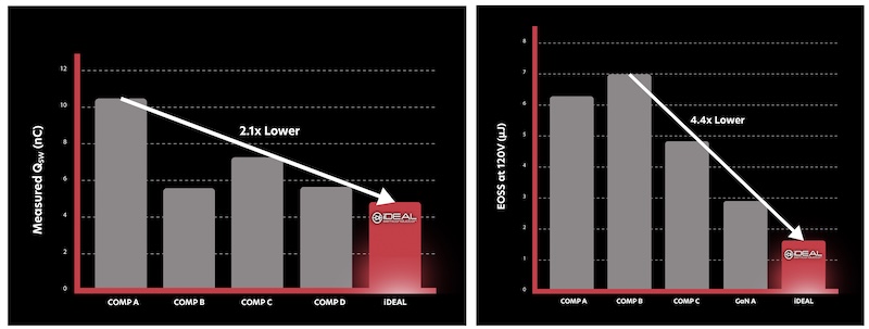
Figure 3. SuperQ vs. competition in measured QSW (left) and EOSS parameters (right). Image used courtesy of Bodo’s Power Systems [PDF]
In brushless direct current (BLDC) motor drives, SuperQ is used for both three-phase inverter switching as well as battery protection. When operated as a battery disconnect switch, it combines industry-leading on-resistance and robustness, including short-circuit current handling up to 700A (see Figure 4).
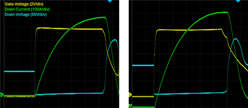
Figure 4. Peak short circuit current to failure for Competitor A (left, 570A) and SuperQ (right, 692A) for similar RDS(on) and silicon area. Green = Drain Current, Blue = Drain-to-Source Voltage, Yellow = Gate-to-Source Voltage. Image used courtesy of Bodo’s Power Systems [PDF]
Another specific example in Telecom/Networking: SuperQ is used as the primary side control MOSFET in a commercially available isolated DC/DC converter operating at 270 kHz in an Active Clamp Forward topology. iDEAL’s SuperQ devices reduce power loss by up to 2 Watts and run as much as 31°C cooler than leading competitors. This translates to improved thermal management and longer system lifespan—benefits made possible by SuperQ’s low resistance and ultralow QSW and EOSS.
On reliability, the SuperQ architecture is engineered to exceed industry standards, with all devices 100% production-screened for unclamped inductive switching (UIS) and delivering energy ratings that surpass application needs.
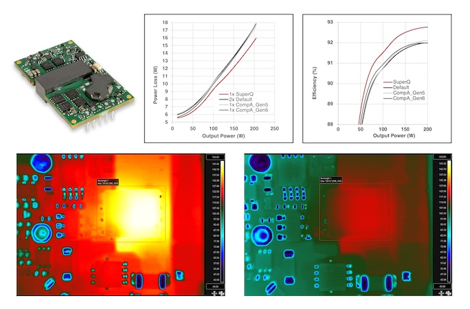
Figure 5. SuperQ performance in an isolated DC/DC converter. Competition 152°C (left), SuperQ 121°C (right). 48Vin, 12Vout, 17A, 5min soak, no forced air cooling. Image used courtesy of Bodo’s Power Systems [PDF]
The safe operating area (SOA) offers wide current/voltage margins and thermal stability, preventing runaway in pulsed operations. Qualified to 175°C junction temperatures, SuperQ endures rigorous JEDEC tests – including HTRB, HTGB, thermal cycling, BHAST, IOL, HTSL, and UHAST – stressed at least twice the standard levels. This level of screening and qualification ensures long-term reliability in even the most demanding industrial, automotive, and data center environments.
Future Implications
The introduction of SuperQ technology represents a significant step forward in extending the performance limits of silicon power devices. By implementing an asymmetrical RESURF structure, SuperQ achieves notable reductions in RDS(on), QSW, and EOSS, while maintaining the advantages of established silicon processes.
SuperQ provides a practical path for system designers seeking higher efficiency and power density without moving away from the mature silicon manufacturing ecosystem. Covering a voltage range from 150 V to 400 V, the platform offers competitive conduction and switching performance for applications such as AI data centers, motor drives, industrial automation, and telecom power systems.
As power conversion requirements continue to grow in complexity and scale, SuperQ demonstrates that silicon still has room for meaningful innovation and performance enhancement.
This article originally appeared in Bodo’s Power Systems [PDF] magazine.